


O Design da Camada Condutiva AZO na Placa do Microcanal
Resumo
Quando a resistividade da camada condutora de AZO está dentro do requisito de resistência MCP, o intervalo do conteúdo de Zn é muito estreito (70-73%) e difícil de controlar. Visando as características da camada condutora de AZO na placa de microcanais, um algoritmo é desenvolvido para ajustar a relação do material condutor ZnO e o material de alta resistência Al2O3. Propomos o conceito de resistência de trabalho do MCP (ou seja, a resistência durante a avalanche de elétrons no microcanal). A resistência de trabalho de AZO-ALD-MCP (placa de microcanais de deposição de camada atômica Al2O3 / ZnO) foi medida pela primeira vez pelo sistema de teste de resistência MCP. Em comparação com o MCP convencional, descobrimos que a resistência do AZO-ALD-MCP no estado operacional e no estado não operacional é muito diferente, e conforme a tensão aumenta, a resistência operacional diminui significativamente. Portanto, propomos um conjunto de métodos analíticos para a camada condutiva. Também propusemos ajustar a proporção do material condutor da camada condutora ALD-MCP para o material de alta resistência sob a condição de resistência de trabalho, e preparamos com sucesso AZO-ALD-MCP de alto ganho. Este projeto abre caminho para encontrar melhores materiais para a camada condutiva do ALD-MCP para melhorar o desempenho do MCP.
Introdução
A placa de microcanais (MCP) é um multiplicador de elétrons composto de matrizes de poros bidimensionais por integração de forma de placa de vidro fina, comprimento de 0,5–5 mm, um diâmetro de 4–40 μm e um ângulo de polarização geralmente 5 ° –13 ° ao normal da superfície da placa; a proporção da área aberta da placa é de até 60%, e a proporção alta do comprimento para o diâmetro em cada poro é de cerca de 20:1 a 100:1 [1].
Como mostrado na Fig. 1, os elétrons incidentes que entram no microcanal colidem com as paredes, fazendo com que elétrons secundários sejam gerados na superfície das paredes do microcanal. Multi-colisões com as paredes do microcanal levarão a um número crescente de elétrons secundários, resultando em uma avalanche de elétrons dentro do microcanal e a emissão de uma nuvem de elétrons da saída do microcanal. Os elétrons secundários serão ainda mais acelerados ao longo do microcanal por uma tensão de polarização. O ganho de MCP é 10 3 –10 4 em uma tensão de trabalho 700–900 V [2,3,4,5,6,7,8,9].
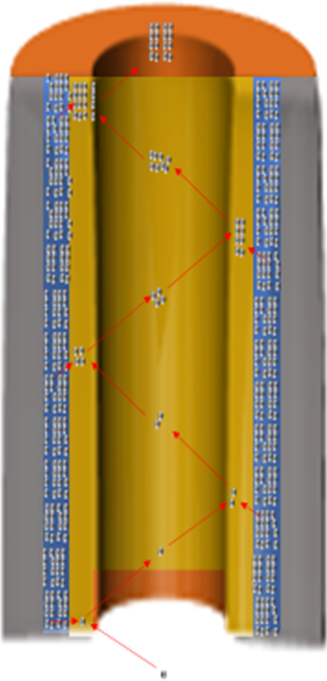
Diagrama de estado de trabalho do MCP
Cada microcanal funciona como um detector e um multiplicador de elétrons. Por ter milhões de microcanais trabalhando de forma independente, o MCP possui as características de alta resolução espacial, alta resolução de tempo e ampla faixa de ganho usada para identificar os fótons, elétrons, nêutrons e íons. O MCP pode se integrar a vários tipos de instrumentos, incluindo detector fotoelétrico, tubos fotomultiplicadores (PMTs), espectrômetro ultravioleta, tubo de raios catódicos, microscópio eletrônico de varredura, visores de emissão de campo, analisador de gás residual, imagens médicas, espectrometria de massa de tempo de voo, noite - óculos de visão, etc. [1, 4, 7,8,9]. A queima de hidrogênio do processo tradicional torna o microcanal adequado para condutividade e coeficiente de emissão de elétrons secundários.
O processo usual de queima de hidrogênio na preparação de um microcanal tem uma série de deficiências:primeiro, o processo de queima de hidrogênio não pode ajustar independentemente a camada condutora e a camada de emissão [10, 11]; em segundo lugar, os elementos de metal pesado (Pb, Bi) levam à poluição ambiental no processo de fundição do vidro com chumbo; terceiro, grandes áreas de MCP ficarão empenadas devido à alta temperatura [8]; quarto, o vidro de chumbo que está sendo usado, a reação de redução de hidrogênio contém K, Rb e outros elementos radioativos, resultando em ruído de fundo [8]; por último, o hidrogênio que permanece nos poros torna-se íons devido à tensão de polarização e eles voam na direção oposta do elétron para destruir o cátodo do instrumento [8, 12].
Os primeiros cientistas propõem uma solução para aumentar a camada condutiva e a camada de emissão na parede do microcanal para substituir o processo de queima de hidrogênio [3]. Muitos métodos de deposição de filme fino são incapazes de crescer um filme uniforme no microcanal com altas razões de comprimento para diâmetro. O laboratório nacional de Argonne propôs o uso de deposição de camada atômica (ALD) para fazer crescer a camada condutiva e a camada de emissão no MCP para obter um filme intacto e uniforme nas paredes do microcanal [4, 13]. Além disso, ALD-MCP resolve as deficiências acima mencionadas. Muitas instituições de pesquisa buscam encontrar materiais competitivos que possam melhorar o desempenho do MCP.
O Argonne National Laboratory seleciona materiais AZO para a camada condutiva ALD-MCP levando em consideração os requisitos de resistência do MCP. Se a resistência for muito alta, a camada condutora não pode repor elétrons para a camada de emissão a tempo e continuamente, o MCP terá ganhos baixos ou até mesmo deixará de operar. Por outro lado, se a resistência for muito baixa, o MCP vai superaquecer, levando a uma quebra [4, 9, 14, 15]. Portanto, o projeto da camada condutiva é importante para um ALD-MCP.
Conforme mostrado na Fig. 2, quando a resistividade da camada condutora de AZO está dentro do requisito de resistência MCP, o conteúdo de Zn permitido está em uma faixa muito estreita (70-73%) [16]. Conseqüentemente, o ganho do MCP é instável e o MCP pode quebrar facilmente. Materiais condutores alternativos como W e Mo no lugar de Zn têm sido estudados [3, 4, 17,18,19]. A reação química de \ ({\ text {WF}} _ {6} \) (\ ({\ text {MoF}} _ {6} \)) e \ ({\ text {H}} _ {2} {\ text {O}} \) é usado para aumentar W (Mo) por ALD. No entanto, usar \ ({\ text {WF}} _ {6} \) ou \ ({\ text {MoF}} _ {6} \) tem duas sérias desvantagens:eles são fortemente corrosivos e contêm impurezas que podem ser difícil de remover durante o processo de produção. Por essas razões, ALD-MCP com esses materiais é caro.
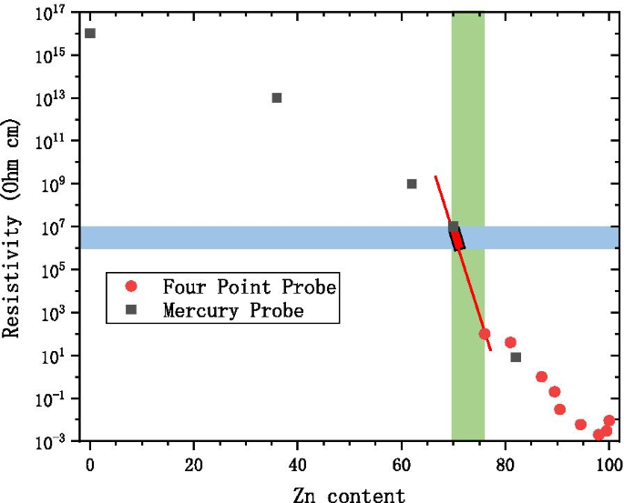
Conteúdo de Zn, Zn / (Zn + A) * 100 (%), área azul como a área de resistência do MCP, área verde como área de mudança AZO, áreas vermelhas como a área necessária para controlar
Em nosso estudo, descobrimos que projetos razoáveis com ZnO e \ ({\ text {Al}} _ {2} {\ text {O}} _ {3} \) podem ser realizados para a camada condutora MCP, sem os desafios enfrentado se W ou Mo for usado e é mais competitivo no preço. Aqui, nomeamos o ALD-MCP com uma camada condutora de AZO como AZO-ALD-MCP.
Nós propomos um algoritmo para ajustar a relação entre o material condutor ZnO e o material de alta resistência \ ({\ text {Al}} _ {2} {\ text {O}} _ {3} \) para obter as características desejadas da camada condutora de AZO.
Propomos o conceito de resistência de trabalho do MCP (ou seja, a resistência durante a avalanche de elétrons no microcanal). Testamos a resistência de trabalho do AZO-ALD-MCP e encontramos duas diferenças entre o AZO-ALD-MCPs e os MCPs convencionais. Observamos que as resistências de trabalho e não de trabalho de AZO-ALD-MCPs e MCPs convencionais são significativamente diferentes. Além disso, a resistência do AZO-ALD-MLP está negativamente correlacionada com a tensão. Nossa proposta (a referência à resistência de trabalho) para ajustar a relação do material condutor e do material de alta resistência fornece uma orientação para nos ajudar na busca de novos materiais a serem usados para a camada condutora ALD-MCP na melhoria do desempenho do MCP no futuro.
Experimental e Métodos
Crescendo ZnO e \ ({\ text {Al}} _ {2} {\ text {O}} _ {3} \) Filme Atômico
A deposição de camada atômica (ALD) é uma tecnologia que alterna precursores e gases reativos à superfície do substrato para adsorção física ou química ou reação de saturação de superfície em uma taxa controlada. O material é depositado sobre o substrato na forma de uma superfície de filme monoatômico. ALD pode produzir um filme contínuo sem orifícios, com excelente cobertura, e pode controlar a espessura e composição do filme atômico [1, 2, 4, 11, 13, 19, 20].
A seguir estão as equações de reação química do uso de ALD para cultivar Al 2 O 3 :
$$ \ begin {alinhados} &{\ text {A}}:{\ text {Substrato}} - {\ text {OH}} ^ {*} + {\ text {Al}} \ left ({{\ text {CH}} _ {3}} \ right) _ {3} \\ &\ quad \ to {\ text {Substrato}} - {\ text {O}} - {\ text {Al}} \ left ({ {\ text {CH}} _ {3}} \ right) _ {2} ^ {*} + {\ text {CH}} _ {4} \ uparrow \\ &{\ text {B}}:{\ texto {Substrato}} - {\ text {O}} - {\ text {Al}} \ left ({{\ text {CH}} _ {3}} \ right) _ {2} ^ {*} + 2 {\ text {H}} _ {2} {\ text {O}} \\ &\ quad \ to {\ text {Substrato}} - {\ text {O}} - {\ text {Al}} \ left ({{\ text {OH}}} \ right) _ {2} ^ {*} + 2 {\ text {CH}} _ {4} \ uparrow \\ &{\ text {C}}:{\ text {Al}} - {\ text {OH}} ^ {*} + {\ text {Al}} \ left ({{\ text {CH}} _ {3}} \ right) _ {3} \\ { } &\ quad \ to {\ text {Al}} - {\ text {O}} - {\ text {Al}} \ left ({{\ text {CH}} _ {3}} \ right) _ { 2} ^ {*} + {\ text {CH}} _ {4} \ uparrow \\ &{\ text {D}}:{\ text {Al}} - {\ text {CH}} _ {3} ^ {*} + {\ text {H}} _ {2} {\ text {O}} \ to {\ text {Al}} - {\ text {OH}} ^ {*} + 2 {\ text { CH}} _ {4} \ uparrow \\ \ end {alinhado} $$
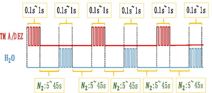
A temperatura da reação é 60-150 ° C. Conforme mostrado na Fig. 3, o tempo e a ordem de crescimento de uma camada de Al 2 O 3 átomo é:
Crescendo Al 2 O 3 e diagrama ZnO
\ ({\ text {TMA}} / {\ text {N}} _ {2} / {\ text {H}} _ {2} {\ text {O}} / {\ text {N}} _ { 2} =0,1 \ sim1 {\ text {s}} / 5 \ sim45 {\ text {s}} / 0,1 \ sim1 {\ text {s}} / 5 \ sim45 {\ text {s}} \).
A seguir estão as equações de reação química para usar ALD para cultivar ZnO:
$$ \ begin {alinhados} &{\ text {E}}:{\ text {Substrato}} - {\ text {OH}} ^ {*} + {\ text {Zn}} \ left ({{\ text {CH}} _ {2} {\ text {CH}} _ {3}} \ right) _ {2} \\ &\ quad \ to {\ text {Substrato}} - {\ text {O}} - {\ text {ZnCH}} _ {2} {\ text {CH}} _ {3} ^ {*} + {\ text {CH}} _ {3} {\ text {CH}} _ {3} \ uparrow \\ &{\ text {F}}:{\ text {Substrato}} - {\ text {O}} - {\ text {ZnCH}} _ {2} {\ text {CH}} _ {3} ^ {*} + {\ text {H}} _ {2} {\ text {O}} \\ &\ quad \ to {\ text {Substrato}} - {\ text {O}} - {\ text { ZnOH}} ^ {*} + {\ text {CH}} _ {3} {\ text {CH}} _ {3} \ uparrow \\ &{\ text {G}}:{\ text {Zn}} - {\ text {OH}} ^ {*} + {\ text {Zn}} \ left ({{\ text {CH}} _ {2} {\ text {CH}} _ {3}} \ right) _ {2} \\ &\ quad \ to {\ text {Zn}} - {\ text {O}} - {\ text {ZnCH}} _ {2} {\ text {CH}} _ {3} ^ {*} + {\ text {CH}} _ {3} {\ text {CH}} _ {3} \ uparrow \\ &{\ text {H}}:{\ text {Zn}} - {\ text {CH}} _ {2} {\ text {CH}} _ {3} ^ {*} + {\ text {H}} _ {2} {\ text {O}} \ to {\ text {Zn} } - {\ text {OH}} ^ {*} + {\ text {CH}} _ {3} {\ text {CH}} _ {3} \ uparrow \\ \ end {alinhados} $$
A temperatura da reação é 60-150 ° C. Conforme mostrado na Fig. 3, o tempo e a ordem de crescimento de uma camada do átomo de ZnO é:
$$ {\ text {DEZ}} / {\ text {N}} _ {2} / {\ text {H}} _ {2} {\ text {O}} / {\ text {N}} _ { 2} =0,1 \ sim1 {\ text {s}} / 5 \ sim45 {\ text {s}} / 0,1 \ sim1 {\ text {s}} / 5 \ sim45 {\ text {s}} {.} $ $
Projeto da Camada Condutiva AZO
A espessura do AZO geralmente varia de 300 a 1000 camadas atômicas. Definimos uma nova regra de operação matemática para projetar as ordens da camada atômica de Al2O3 e ZnO a fim de ajustar a proporção do material condutor ZnO e do material de alta resistência Al2O3.
$$ \ left (\ begin {array} {* {20} c} {{\ text {mA}}} \\ {{\ text {mB}}} \\ \ vdots \\ \ end {array} \ right ) ={\ text {m}} \ left (\ begin {array} {* {20} c} {\ text {A}} \\ {\ text {B}} \\ \ vdots \\ \ end {array } \ right) $$ (1) $$ \ begin {align} &{\ text {A}} \ left (\ begin {array} {* {20} c} {\ text {a}} \\ {\ texto {b}} \\ \ vdots \\ \ end {array} \ right) + {\ text {B}} \ left (\ begin {array} {* {20} c} {\ text {c}} \ \ {\ text {d}} \\ \ vdots \\ \ end {array} \ right) + {\ text {C}} \ left (\ begin {array} {* {20} c} {\ text {e }} \\ {\ text {f}} \\ \ vdots \\ \ end {array} \ right) \ ldots \\ &\ quad =\ left (\ begin {array} {* {20} c} {\ text {A}} \\ {\ text {B}} \\ \ vdots \\ \ end {array} \ right) \ left [\ left (\ begin {array} {* {20} c} {\ text { a}} \\ {\ text {b}} \\ \ vdots \\ \ end {array} \ right) \ left (\ begin {array} {* {20} c} {\ text {c}} \\ {\ text {d}} \\ \ vdots \\ \ end {array} \ right) \ left (\ begin {array} {* {20} c} {\ text {e}} \\ {\ text {f }} \\ \ vdots \\ \ end {array} \ right) \ ldots \ right] =\ left (\ begin {array} {* {20} c} {{\ text {Aa}} + {\ text { Bc}} + {\ text {Ce}} + \ ldots} \\ {{\ text {Ab}} + {\ text {Bd}} + {\ text {Cf}} + \ ldots} \\ \ vdots \\ \ end {array} \ right) \\ \ end {alinhado} $$ (2)
A operação matemática foi denominada operação WYM. A operação WYM tem duas propriedades e uma fórmula.
Propriedade WYM 1:
$$ \ begin {alinhado} &\ left ({\ begin {array} {* {20} c} {\ text {m}} \\ {\ text {n}} \\ \ end {array}} \ right ) \ left [{\ left ({\ begin {array} {* {20} c} {\ text {a}} \\ {\ text {b}} \\ \ end {array}} \ right) \ left ({\ begin {array} {* {20} c} {\ text {c}} \\ {\ text {d}} \\ \ end {array}} \ right)} \ right] \ left [{\ esquerda ({\ begin {array} {* {20} c} {\ text {e}} \\ {\ text {f}} \\ \ end {array}} \ right) \ left ({\ begin {array } {* {20} c} {\ text {g}} \\ {\ text {h}} \\ \ end {array}} \ right)} \ right] \ left [{\ left ({\ begin { array} {* {20} c} {\ text {i}} \\ {\ text {j}} \\ \ end {array}} \ right) \ left ({\ begin {array} {* {20} c} {\ text {k}} \\ {\ text {l}} \\ \ end {array}} \ right)} \ right] \ ldots \\ &\ quad =\ left ({\ begin {array} {* {20} c} {\ text {m}} \\ {\ text {n}} \\ \ end {array}} \ right) \ left \ {{\ left ({\ begin {array} {* {20} c} {\ text {a}} \\ {\ text {b}} \\ \ end {array}} \ right) \ left [{\ left ({\ begin {array} {* {20} c} {\ text {e}} \\ {\ text {f}} \\ \ end {array}} \ right) \ left ({\ begin {array} {* {20} c} {\ text {g }} \\ {\ text {h}} \\ \ end {array}} \ right)} \ right], \ left ({\ beg em {array} {* {20} c} {\ text {c}} \\ {\ text {d}} \\ \ end {array}} \ right) \ left [{\ left ({\ begin {array } {* {20} c} {\ text {e}} \\ {\ text {f}} \\ \ end {array}} \ right) \ left ({\ begin {array} {* {20} c } {\ text {g}} \\ {\ text {h}} \\ \ end {array}} \ right)} \ right]} \ right \} \ left [{\ left ({\ begin {array} {* {20} c} {\ text {i}} \\ {\ text {j}} \\ \ end {array}} \ right) \ left ({\ begin {array} {* {20} c} {\ text {k}} \\ {\ text {l}} \\ \ end {array}} \ right)} \ right] \ ldots \\ &\ quad =\ left ({\ begin {array} {* {20} c} {\ text {m}} \\ {\ text {n}} \\ \ end {array}} \ right) \ left [{\ left ({\ begin {array} {* {20} c} {\ text {a}} \\ {\ text {b}} \\ \ end {array}} \ right) \ left ({\ begin {array} {* {20} c} {\ text {c }} \\ {\ text {d}} \\ \ end {array}} \ right)} \ right] \ left \ {{\ left ({\ begin {array} {* {20} c} {\ text {e}} \\ {\ text {f}} \\ \ end {array}} \ right) \ left [{\ left ({\ begin {array} {* {20} c} {\ text {i} } \\ {\ text {j}} \\ \ end {array}} \ right) \ left ({\ begin {array} {* {20} c} {\ text {k}} \\ {\ text { l}} \\ \ end {array}} \ right)} \ right], \ left ({\ begin {array} {* {20} c} {\ te xt {g}} \\ {\ text {h}} \\ \ end {array}} \ right) \ left [{\ left ({\ begin {array} {* {20} c} {\ text {i }} \\ {\ text {j}} \\ \ end {array}} \ right) \ left ({\ begin {array} {* {20} c} {\ text {k}} \\ {\ text {l}} \\ \ end {array}} \ right)} \ right]} \ right \} \ ldots \\ \ end {alinhados} $$
Propriedade 2 do WYM:
$$ \ begin {alinhados} &{\ text {A}} \ left ({\ begin {array} {* {20} c} {\ text {m}} \\ {\ text {n}} \\ \ end {array}} \ right) \ left [{\ left ({\ begin {array} {* {20} c} {\ text {a}} \\ {\ text {b}} \\ \ end {array }} \ right) \ left ({\ begin {array} {* {20} c} {\ text {c}} \\ {\ text {d}} \\ \ end {array}} \ right)} \ direita] \ esquerda [{\ esquerda ({\ begin {array} {* {20} c} {\ text {e}} \\ {\ text {f}} \\ \ end {array}} \ right) \ esquerda ({\ begin {array} {* {20} c} {\ text {g}} \\ {\ text {h}} \\ \ end {array}} \ right)} \ right] \ ldots \\ &\ quad =\ left ({\ begin {array} {* {20} c} {{\ text {Am}}} \\ {{\ text {An}}} \\ \ end {array}} \ right ) \ left [{\ left ({\ begin {array} {* {20} c} {\ text {a}} \\ {\ text {b}} \\ \ end {array}} \ right) \ left ({\ begin {array} {* {20} c} {\ text {c}} \\ {\ text {d}} \\ \ end {array}} \ right)} \ right] \ left [{\ esquerda ({\ begin {array} {* {20} c} {\ text {e}} \\ {\ text {f}} \\ \ end {array}} \ right) \ left ({\ begin {array } {* {20} c} {\ text {g}} \\ {\ text {h}} \\ \ end {array}} \ right)} \ right] \ ldots \\ &\ quad =\ left ( {\ begin {array} {* {20} c} {\ text {m}} \\ {\ text {n}} \\ \ end {a rray}} \ right) \ left [{{\ text {A}} \ left ({\ begin {array} {* {20} c} {\ text {a}} \\ {\ text {b}} \ \ \ end {array}} \ right), {\ text {A}} \ left ({\ begin {array} {* {20} c} {\ text {c}} \\ {\ text {d}} \\ \ end {array}} \ right)} \ right] \ left [{\ left ({\ begin {array} {* {20} c} {\ text {e}} \\ {\ text {f} } \\ \ end {array}} \ right) \ left ({\ begin {array} {* {20} c} {\ text {g}} \\ {\ text {h}} \\ \ end {array }} \ right)} \ right] \ ldots \\ &\ quad =\ left ({\ begin {array} {* {20} c} {\ text {m}} \\ {\ text {n}} \ \ \ end {array}} \ right) \ left [{\ left ({\ begin {array} {* {20} c} {\ text {a}} \\ {\ text {b}} \\ \ end {array}} \ right) \ left ({\ begin {array} {* {20} c} {\ text {c}} \\ {\ text {d}} \\ \ end {array}} \ right) } \ right] \ left [{{\ text {A}} \ left ({\ begin {array} {* {20} c} {\ text {e}} \\ {\ text {f}} \\ \ end {array}} \ right), {\ text {A}} \ left ({\ begin {array} {* {20} c} {\ text {g}} \\ {\ text {h}} \\ \ end {array}} \ right)} \ right] \ ldots \\ \ end {alinhados} $$
Fórmula WYM:
$$ \ begin {alinhado} &\ left (\ begin {array} {* {20} c} {\ text {a}} \\ {\ text {b}} \\ \ vdots \\ \ end {array} \ right) =\ left (\ begin {array} {* {20} c} {{\ text {A}} + \ frac {{\ text {X}}} {{\ text {Y}}}} \ \ {\ text {b}} \\ \ vdots \\ \ end {array} \ right) \ propto {\ text {Y}} \ left (\ begin {array} {* {20} c} {{\ text {A}} + \ frac {{\ text {X}}} {{\ text {Y}}}} \\ {\ text {b}} \\ \ vdots \\ \ end {array} \ right) =\ left ({\ begin {array} {* {20} c} {{\ text {Y}} - {\ text {X}}} \\ {\ text {X}} \\ \ end {array}} \ right) \ left [\ left (\ begin {array} {* {20} c} {\ text {A}} \\ {\ text {b}} \\ \ vdots \\ \ end {array} \ right ) \ left (\ begin {array} {* {20} c} {{\ text {A}} + 1} \\ {\ text {b}} \\ \ vdots \\ \ end {array} \ right) \ right] \\ &\ left (\ begin {array} {* {20} c} {\ text {a}} \\ {\ text {b}} \\ \ vdots \\ \ end {array} \ right ) =\ left (\ begin {array} {* {20} c} {\ text {a}} \\ {{\ text {B}} + \ frac {{\ text {X}}} {{\ text {Y}}}} \\ \ vdots \\ \ end {array} \ right) \ propto {\ text {Y}} \ left (\ begin {array} {* {20} c} {\ text {a} } \\ {{\ text {B}} + \ frac {{\ text {X}}} {{\ text {Y}}}} \\ \ vdots \\ \ end {array} \ right) =\ left ({\ begin {array} {* {20} c} {{\ text {Y}} - {\ text {X}}} \\ {\ text {X}} \\ \ end {array}} \ right) \ left [\ left (\ begin {array} {* {20} c} {\ text {a}} \\ {\ text {B}} \\ \ vdots \\ \ end {array} \ right ) \ left (\ begin {array} {* {20} c} {\ text {a}} \\ {{\ text {B}} + 1} \\ \ vdots \\ \ end {array} \ right) \ right] \\ \ end {alinhado} $$
Observe que as letras minúsculas representam números reais, enquanto as letras maiúsculas representam inteiros. Nos exemplos 1 e 2, mostramos a execução da operação.
Exemplo 1
$$ \ left ({\ begin {array} {* {20} c} {{\ text {ZnO}}} \\ {{\ text {Al}} _ {2} {\ text {O}} _ { 3}} \\ \ end {array}} \ right) =\ left ({\ begin {array} {* {20} c} {4 + \ frac {1} {2}} \\ 1 \\ \ end {array}} \ right) \ propto \ left ({\ begin {array} {* {20} c} 1 \\ 1 \\ \ end {array}} \ right) \ left [{\ left ({\ begin {array} {* {20} c} 4 \\ 1 \\ \ end {array}} \ right) \ left ({\ begin {array} {* {20} c} 5 \\ 1 \\ \ end { array}} \ right)} \ right] =\ left ({\ begin {array} {* {20} c} 4 \\ 1 \\ \ end {array}} \ right) + \ left ({\ begin { array} {* {20} c} 5 \\ 1 \\ \ end {array}} \ right) $$
A operação é interpretada como tendo dois esquemas:\ (\ left ({\ begin {array} {* {20} c} 4 \\ 1 \\ \ end {array}} \ right) \) e \ (\ left ( {\ begin {array} {* {20} c} 5 \\ 1 \\ \ end {array}} \ right) \). Para o primeiro esquema, aumente 4 vezes a camada atômica de ZnO e uma camada atômica de Al2O3. Para o segundo esquema, aumente 5 vezes a camada atômica de ZnO e uma camada atômica de Al2O3. Se repetirmos esses dois esquemas duas vezes, obteremos a estrutura mostrada na Fig. 4.
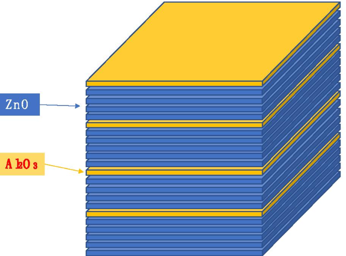
Diagrama esquemático de ZnO e Al 2 O 3 sequência de crescimento
Um uso mais complicado das regras de operação é mostrado no Exemplo 2, da seguinte maneira:
$$ \ begin {alinhados} &\ left ({\ begin {array} {* {20} c} {{\ text {ZnO}}} \\ {{\ text {Al}} _ {2} {\ text {O}} _ {3}} \\ \ end {array}} \ right) =\ left ({\ begin {array} {* {20} c} {4,71} \\ 1 \\ \ end {array} } \ right) =\ left ({\ begin {array} {* {20} c} {4 + 0.71} \\ 1 \\ \ end {array}} \ right) \\ &\ frac {2} {3 } =0,666 <0,71 <\ frac {3} {4} =0,75 \\ &\ left ({\ begin {array} {* {20} c} E \\ F \\ \ end {array}} \ right) \ left [{\ left ({\ begin {array} {* {20} c} {4 + \ frac {2} {3}} \\ 1 \\ \ end {array}} \ right) \ left ({ \ begin {array} {* {20} c} {4 + \ frac {3} {4}} \\ 1 \\ \ end {array}} \ right)} \ right] \\ &\ quad =E \ esquerda ({\ begin {array} {* {20} c} {4 + \ frac {2} {3}} \\ 1 \\ \ end {array}} \ right) + F \ left ({\ begin { array} {* {20} c} {4 + \ frac {3} {4}} \\ 1 \\ \ end {array}} \ right) =\ left ({\ begin {array} {* {20} c} {4E + 4F + \ frac {2} {3} E + \ frac {3} {4} F} \\ {E + F} \\ \ end {array}} \ right) \\ &\ quad =E + F \ left ({\ begin {array} {* {20} c} {4 + \ frac {{\ frac {2} {3} E + \ frac {3} {4} F}} {E + F}} \\ 1 \\ \ end {array}} \ right) \ propto \ left ({\ begin {array} {* {20} c} {4 + \ frac {{\ frac {2} {3} E + \ frac {3} {4} F}} {E + F}} \\ 1 \\ \ end {array}} \ right) =\ left ({\ begin {array} {* {20} c} {4,71} \\ 1 \\ \ end {array}} \ right) \\ &\ frac {{\ frac {2} { 3} E + \ frac {3} {4} F}} {E + F} =0,71 \ Rightarrow {\ text {E}} =12, {\ text {F}} =13 \\ &\ left ({ \ begin {array} {* {20} c} E \\ F \\ \ end {array}} \ right) =\ left ({\ begin {array} {* {20} c} {12} \\ { 13} \\ \ end {array}} \ right) =12 \ left ({\ begin {array} {* {20} c} 1 \\ {1 \ frac {1} {12}} \\ \ end { array}} \ right) =\ left ({\ begin {array} {* {20} c} {11} \\ 1 \\ \ end {array}} \ right) \ left [{\ left ({\ begin {array} {* {20} c} 1 \\ 1 \\ \ end {array}} \ right) \ left ({\ begin {array} {* {20} c} 1 \\ 2 \\ \ end { array}} \ right)} \ right] \\ &\ left ({\ begin {array} {* {20} c} E \\ F \\ \ end {array}} \ right) \ left [{\ left ({\ begin {array} {* {20} c} {4 + \ frac {2} {3}} \\ 1 \\ \ end {array}} \ right), \ left ({\ begin {array} {* {20} c} {4 + \ frac {3} {4}} \\ 1 \\ \ end {array}} \ right)} \ right] \\ &\ quad =\ left ({\ begin { array} {* {20} c} E \\ F \\ \ end {array}} \ right) \ left [{ \ left ({\ begin {array} {* {20} c} 1 \\ 2 \\ \ end {array}} \ right) \ left [{\ left ({\ begin {array} {* {20} c } 4 \\ 1 \\ \ end {array}} \ right) \ left ({\ begin {array} {* {20} c} 5 \\ 1 \\ \ end {array}} \ right)} \ right ], \ left ({\ begin {array} {* {20} c} 1 \\ 3 \\ \ end {array}} \ right) \ left [{\ left ({\ begin {array} {* {20 } c} 4 \\ 1 \\ \ end {array}} \ right) \ left ({\ begin {array} {* {20} c} 5 \\ 1 \\ \ end {array}} \ right)} \ right]} \ right] \\ &\ left ({\ begin {array} {* {20} c} {4.71} \\ 1 \\ \ end {array}} \ right) \ propto \ left ({\ begin {array} {* {20} c} {12} \\ {13} \\ \ end {array}} \ right) \ left [{\ left ({\ begin {array} {* {20} c} 1 \\ 2 \\ \ end {array}} \ right) \ left ({\ begin {array} {* {20} c} 1 \\ 3 \\ \ end {array}} \ right)} \ right] \ left [{\ left ({\ begin {array} {* {20} c} 4 \\ 1 \\ \ end {array}} \ right) \ left ({\ begin {array} {* {20} c } 5 \\ 1 \\ \ end {array}} \ right)} \ right] =\ left ({\ begin {array} {* {20} c} {11} \\ 1 \\ \ end {array} } \ right) \ left [{\ left ({\ begin {array} {* {20} c} 1 \\ 1 \\ \ end {array}} \ right) \ left ({\ begin {array} {* {20} c } 1 \\ 2 \\ \ end {array}} \ right)} \ right] \ left [{\ left ({\ begin {array} {* {20} c} 1 \\ 2 \\ \ end {array }} \ right) \ left ({\ begin {array} {* {20} c} 1 \\ 3 \\ \ end {array}} \ right)} \ right] \ left [{\ left ({\ begin {array} {* {20} c} 4 \\ 1 \\ \ end {array}} \ right) \ left ({\ begin {array} {* {20} c} 5 \\ 1 \\ \ end { array}} \ right)} \ right] \\ \ end {alinhados} $$
Plano 1 :\ (\ left ({\ begin {array} {* {20} c} {4,71} \\ 1 \\ \ end {array}} \ right) \ propto 12 \ left [{\ left ({\ begin { array} {* {20} c} 4 \\ 1 \\ \ end {array}} \ right) + 2 \ left ({\ begin {array} {* {20} c} 5 \\ 1 \\ \ end {array}} \ right)} \ right] + 13 \ left [{\ left ({\ begin {array} {* {20} c} 4 \\ 1 \\ \ end {array}} \ right) + 3 \ left ({\ begin {array} {* {20} c} 5 \\ 1 \\ \ end {array}} \ right)} \ right] \).
Plano 2 \ (\ left ({\ begin {array} {* {20} c} {4,71} \\ 1 \\ \ end {array}} \ right) \ propto 11 \ left [{\ left [{\ left ({ \ begin {array} {* {20} c} 4 \\ 1 \\ \ end {array}} \ right) + 2 \ left ({\ begin {array} {* {20} c} 5 \\ 1 \ \ \ end {array}} \ right)} \ right] + \ left [{\ left ({\ begin {array} {* {20} c} 4 \\ 1 \\ \ end {array}} \ right) + 3 \ left ({\ begin {array} {* {20} c} 5 \\ 1 \\ \ end {array}} \ right)} \ right]} \ right] + \ left [{\ left [{ \ left ({\ begin {array} {* {20} c} 4 \\ 1 \\ \ end {array}} \ right) + 2 \ left ({\ begin {array} {* {20} c} 5 \\ 1 \\ \ end {array}} \ right)} \ right] + 2 \ left [{\ left ({\ begin {array} {* {20} c} 4 \\ 1 \\ \ end {array }} \ right) + 3 \ left ({\ begin {array} {* {20} c} 5 \\ 1 \\ \ end {array}} \ right)} \ right]} \ right] \).
No Exemplo 2, a operação no Plano 1 pode ser interpretada da seguinte forma:
Esquema 1 ALD cresce 4 vezes o processo de crescimento da camada atômica de ZnO e um processo de crescimento da camada atômica \ ({\ text {Al}} _ {2} {\ text {O}} _ {3} \); ALD cresce 5 vezes o processo de crescimento da camada atômica de ZnO e um processo de crescimento da camada atômica \ ({\ text {Al}} _ {2} {\ text {O}} _ {3} \) e repita duas vezes.
Esquema 2 ALD cresce 4 vezes o processo de crescimento da camada atômica de ZnO e um processo de crescimento da camada atômica \ ({\ text {Al}} _ {2} {\ text {O}} _ {3} \); ALD cresce 5 vezes o processo de crescimento da camada atômica de ZnO e um processo de crescimento da camada atômica \ ({\ text {Al}} _ {2} {\ text {O}} _ {3} \) e repita três vezes.
Repita o esquema 1 por 12 vezes e o esquema 2 por 13 vezes.
A interpretação da operação no Plano 2 segue a mesma linha do Plano 1.
Teste de resistência da placa do microcanal
Conforme mostrado na Fig. 5a, usamos a tecnologia de deposição de camada atômica para aumentar a camada condutora de AZO e a camada de emissão \ ({\ text {Al}} _ {2} {\ text {O}} _ {3} \) paredes de microcanais das matrizes de poros bidimensionais. E então usamos a tecnologia de evaporação térmica para aumentar a camada de eletrodo Ni – Cr em ambos os lados do MCP [2, 4] e colocar o anel do eletrodo em ambos os lados do MCP. Fazendo os preparativos para o acima exposto, testamos diretamente a resistência ALD-MCP. Nesta condição, definimos a resistência MCP correspondente como a resistência não funcional do MCP. Usamos um eletrômetro Keithley modelo 6517B para medir a resistência não funcional do MCP em um 10 −3 –10 −5 Vácuo Pa [1, 4, 13].
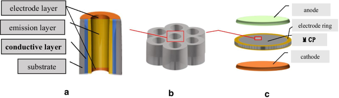
Diagrama esquemático de teste de resistência ALD-MCP
Conforme mostrado na Fig. 5c, usamos um canhão de elétrons como cátodo e uma tela de fósforo como ânodo. O canhão de elétrons fornece elétrons incidentes ao MCP e a tela de fósforo recebe a saída de elétrons do MCP. Além disso, quando o MCP estiver em operação, a tela de fósforo de alta tensão emitirá luz verde para detectar a uniformidade do MCP [1, 21].
Conforme mostrado na Fig. 1, usamos um canhão de elétrons que fornece 100 pA como entrada do MCP para medir a corrente. Devido a um número crescente de elétrons secundários, haverá uma condição em que a camada de emissão perderá uma grande quantidade de cargas e a camada condutiva fornecerá continuamente um fluxo de cargas para a camada de emissão. Nesta condição, definimos a resistência do MCP correspondente como a resistência de trabalho do MCP. O ambiente de vácuo da resistência de trabalho é 10 −3 –10 −5 Pa.
Resultado e discussão
A imagem SEM transversal da amostra AZO-ALD-MCP é mostrada na Fig. 6. Projetamos uma série de camadas condutoras de AZO conforme mostrado na Tabela 1 e suas resistências de trabalho e não-trabalho correspondentes na Fig. 7. No mesma figura, nós também mostramos as resistências de trabalho e não de trabalho de um MCP convencional. Em comparação com a resistência não operacional do AZO-ALD-MCP, a resistência operacional do AZO-ALD-MCP é significativamente reduzida. No entanto, não há diferença significativa entre a resistência de trabalho e a resistência de não trabalho de um MCP convencional. À medida que a tensão aumenta, a resistência de trabalho do AZO-ALD-MCP é significativamente menor do que a de um MCP convencional. Sob a mesma condição de tensão, as resistências de trabalho e não de trabalho do AZO-ALD-MCP são estáveis. Acreditamos que haja duas razões principais para as características acima mencionadas.
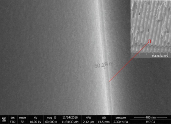
Imagem SEM transversal do AZO-ALD-MCP
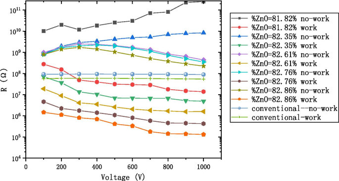
A resistência de trabalho e a resistência de não trabalho com o diagrama de tensão no AZO-ALD-MCP na relação diferente e convencional-MCP
De acordo com a fórmula [21],
$$ R _ {{{\ text {MCP}}}} =R_ {0} \ exp \ left [{- \ beta_ {T} \ left ({T _ {{{\ text {MCP}}}} - T_ { 0}} \ right)} \ right] $$
comparado ao vidro de chumbo, o AZO é um material com coeficiente de temperatura negativo (NTC) maior, portanto a resistência será menor na mesma temperatura e resistência inicial. No processo de geração de ganho, o AZO é bombardeado por elétrons incidentes em alta tensão, gerando assim mais pares elétron-buraco, resultando em um aumento na corrente.
Definimos a proporção de resistência não operacional para resistência operacional para descrever a estabilidade da resistência do material:
$$ \ kappa_ {R} =\ frac {{R_ {n}}} {{R_ {w}}} $$
A Figura 8 mostra que o \ (\ kappa_ {R} \) do AZO-ALD-MCP é cerca de 10 2 –10 3 vezes, e o \ (\ kappa_ {R} \) do convencional-MCP é cerca de 2–3 vezes. Isso mostra que a alteração da resistência do AZO-ALD-MCP é mais óbvia; portanto, o antigo conceito de resistência não operacional como a definição de resistência MCP deve ser substituído pela resistência operacional.
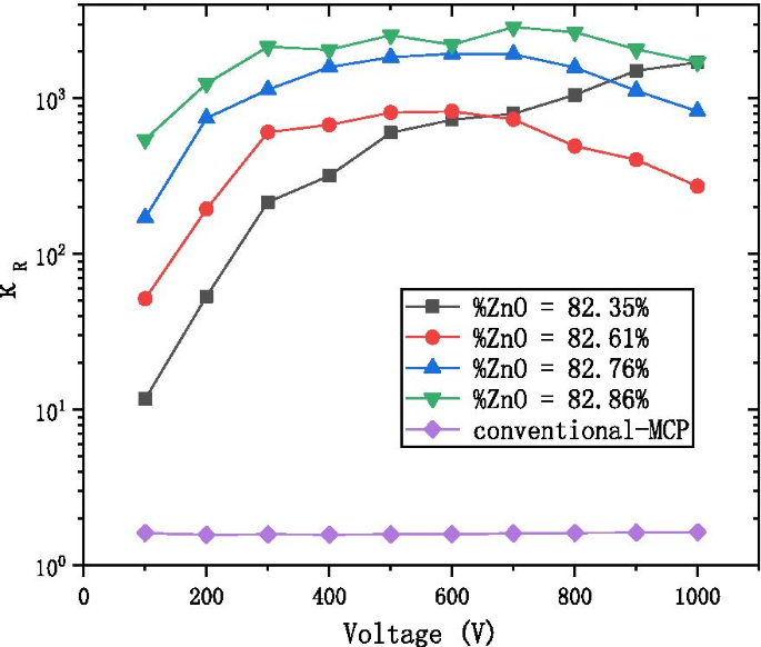
O K R com o diagrama de tensão na relação diferente de AZO-ALD-MCP
A Figura 9 mostra a relação \ (L_ {R} \) da resistência do projeto do material “adjacente” em relação à tensão de operação. A proporção \ (L_ {R} \) é definida como:
$$ L_ {R} =\ frac {{R \ left ({4 + \ frac {N - 1} {N}} \ right)}} {{R \ left ({4 + \ frac {N} {N + 1}} \ right)}} $$
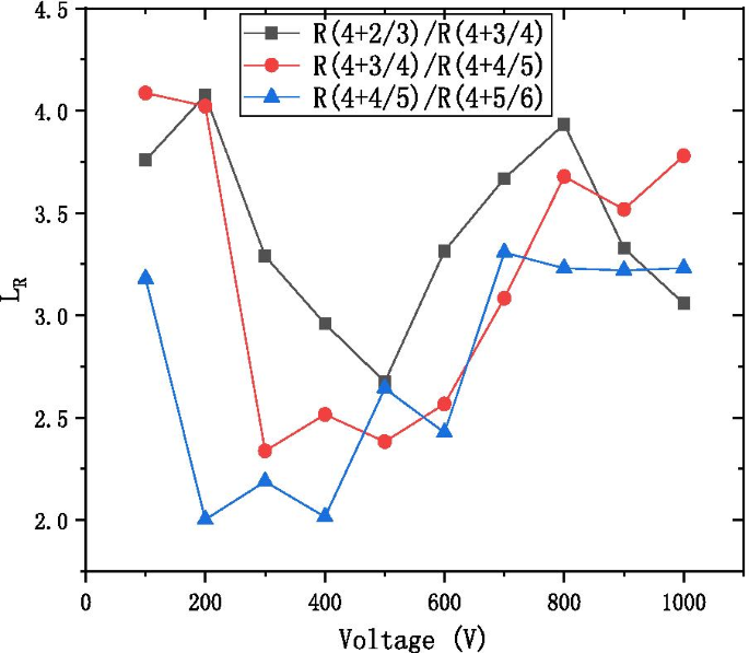
The resistance of the step length LR with the voltage diagram at the different ratio of the working resistance of neighbor formula
Onde
$$\left( {\begin{array}{*{20}c} {{\text{ZnO}}} \\ {{\text{Al}}_{2} {\text{O}}_{3} } \\ \end{array} } \right) =\left( {\begin{array}{*{20}c} {4 + \frac{N - 1}{N}} \\ 1 \\ \end{array} } \right) =\left( {\begin{array}{*{20}c} 1 \\ {N - 1} \\ \end{array} } \right)\left[ {\left( {\begin{array}{*{20}c} 4 \\ 1 \\ \end{array} } \right)\left( {\begin{array}{*{20}c} 5 \\ 1 \\ \end{array} } \right)} \right]$$
e
$$\left( {\begin{array}{*{20}c} {{\text{ZnO}}} \\ {{\text{Al}}_{2} {\text{O}}_{3} } \\ \end{array} } \right) =\left( {\begin{array}{*{20}c} {4 + \frac{N}{N + 1}} \\ 1 \\ \end{array} } \right) =\left( {\begin{array}{*{20}c} 1 \\ N \\ \end{array} } \right)\left[ {\left( {\begin{array}{*{20}c} 4 \\ 1 \\ \end{array} } \right)\left( {\begin{array}{*{20}c} 5 \\ 1 \\ \end{array} } \right)} \right]$$
As can be observed from Fig. 9, the LR value ranges from 2 to 4.5 to adjust ratio of conductive material ZnO and high resistance material \({\text{Al}}_{2} {\text{O}}_{3}\). And it proves the feasibility of WYM operation to design laminated materials.
Figure 10 shows the working resistance with respect to the percentage of ZnO cycles (%ZnO), where %ZnO is defined to be:
$${\text{\% ZnO}} =\frac{{{\text{ZnO}}}}{{{\text{ZnO}} + {\text{Al}}_{2} {\text{O}}_{3} }}{*}100\left( {\text{\% }} \right)$$

The working resistance with the percentage of ZnO cycles diagram at the different voltage
under various voltage conditions, ranging from 100 to 1000 V. It decreases that the working resistance under the same voltage with the increase in the percentage of ZnO cycles. It can be the same that the working resistance under different the percentage of ZnO cycles and under the different condition of voltage. Therefore, the AZO-ALD-MCP of different formulations works under its specific voltage to meet the MCP resistance index.
We define the ratio of the resistance difference under the different condition of voltage and the voltage difference to describe the effect of the voltage on the resistance of MCP:
$$r =\left| {\frac{{R_{U} - R_{V} }}{U - V}} \right| =\left| {\frac{{R_{1000v} - R_{100v} }}{1000 - 100}} \right|$$
Figure 11 shows that the effect of the voltage on the resistance of AZO-ALD-MCP decreased and gradually stabilized with the increase in the percentage of ZnO cycles. Therefore, the preparation of AZO-ALD-MCP should try to choose a formula with a large percentage of ZnO cycles.

The r with the percentage of ZnO cycles diagram at the working state
Based on the above analysis, we have put forward the reference to the working resistance for the conductive layer of ALD-MCP. As shown in Fig. 5a, we design the AZO conductive layer of AZO-MCP by using the WYM operation and temperature adjustment based on the working resistance. We use atomic layer deposition technology to grow the \({\text{Al}}_{2} {\text{O}}_{3}\) emission layer on microchannel wall of the two-dimensional pore arrays [3, 11, 22]. In Fig. 12a, the gain from our AZO-ALD-MCP is compared to that of a conventional MCP under different voltages. As can be observed, our preparation method of the AZO-ALD-MCP provides a larger gain than that of a conventional MCP. Figure 12b shows the phosphor screen with uniform green light under high pressure, thus proving the uniformity of the material deposited on the wall of each microchannel and the uniformity of the AZO-ALD-MCP field of view.

The gain with the voltage diagram at the AZO-ALD-MCP and conventional-MCP
Conclusão
We defined the working and non-working resistance of the microchannel plate. Aiming at the required resistivity of the microchannel plate in the region with extremely narrow zinc content requirement (70–73%), an algorithm for growing the AZO conductive layer is proposed. Compared with the conventional MCP, we found a large difference between the working and non-working resistance and there is also a huge difference under different voltages. Therefore, we analyze the data by defining \(\kappa_{R} ,L_{R} ,\% {\text{ZnO}},r\). MCP should try to choose a formula with a large percentage of ZnO cycles. We recommend using the working resistance as an ALD-MCP resistance indicator in industrial production. Building on our results as described in this work, our studies will help to find even better materials as the conductive layer for the ALD-MCP.
Histórico de alterações
Nanoestruturas de MgO dopadas com óxido de grafeno para degradação de corante altamente eficiente e ação bactericida
Efeito antibacteriano duplo de nanofibras compostas de curcumina por eletrofiação in situ para esterilizar bactérias resistentes a medicamentos
Nanomateriais
- A função do design auxiliado por computador (CAD) na impressão 3D
- Os desafios do design de produto
- O Tetrodo
- O que é design de sistema incorporado:etapas no processo de design
- Design Generativo e Impressão 3D:A Fabricação do Amanhã
- Desenho industrial na era da IoT
- Otimizando a linha de alimentação RF no design de PCB
- Pacote de design PCB leva para a nuvem
- Os benefícios da prototipagem de PCBs
- Conheça o significado da BOM no projeto de PCB