


O Projeto da Camada de Emissão para Multiplicadores de Elétrons
Resumo
O ganho dos multiplicadores de elétrons está intimamente relacionado ao coeficiente de emissão de elétrons secundários (SEE) dos materiais da camada de emissão. O SEE está intimamente relacionado à espessura da camada de emissão. Se a camada de emissão for fina, o baixo SEE causa o baixo ganho dos multiplicadores de elétrons. Se a camada de emissão for espessa, a camada condutiva não pode complementar a carga na camada de emissão, o ganho do amplificador eletrônico também é baixo. Os multiplicadores de elétrons geralmente escolhem Al 2 O 3 e filme de MgO como a camada de emissão devido ao alto nível SEE. Deliquescência fácil de MgO em Mg (OH) 2 Mg 2 (OH) 2 CO 3 e MgCO 3 resultando no nível SEE mais baixo. O nível SEE de Al 2 O 3 é menor que MgO, mas Al 2 O 3 é estável. Projetamos um sistema esférico para testar o nível SEE de materiais e propusemos o uso de elétrons secundários de baixa energia em vez de feixe de elétrons de baixa energia para neutralização para medir o nível SEE de Al 2 O 3 , MgO, MgO / Al 2 O 3 , Al 2 O 3 / MgO, e controlar com precisão a espessura do filme usando deposição de camada atômica. Propomos comparar o SEE sob a energia dos elétrons incidentes adjacentes para particionar o valor SEE do material e obter quatro fórmulas empíricas para a relação entre o SEE e a espessura. Uma vez que os principais materiais que causam a diminuição no SEE são Mg 2 (OH) 2 CO 3 e MgCO 3 , usamos a concentração atômica do elemento C medida por XPS para estudar a profundidade deliquescente do material. Propomos usar o conceito de camada de transição para interpretação SEE de materiais multicamadas. Por meio de experimentos e cálculos, propomos uma nova camada de emissão para multiplicadores de elétrons, incluindo 2–3 nm de Al 2 O 3 camada tampão, camada de corpo principal de MgO de 5–9 nm, Al de 1 nm 2 O 3 camada protetora ou 0,3 nm Al 2 O 3 camada de aprimoramento. Preparamos esta camada de emissão para placa de microcanais (MCP), o que melhorou significativamente o ganho de MCP. Também podemos aplicar esta nova camada de emissão para canalizar o multiplicador de elétrons e separar o multiplicador de elétrons.
Introdução
O coeficiente de emissão de elétrons secundários (SEE) de um material é definido como a razão entre o número de elétrons secundários emitidos e o número de elétrons incidentes no material. O campo de aplicação dos elétrons secundários é muito amplo, dividido principalmente em campo de multiplicação de elétrons, campo de composição de superfície de material e análise de estrutura e campo de supressão de micro-descarga. O campo de multiplicação de elétrons inclui multiplicador de elétrons de canal (CEM), placa de microcanais (MCP), multiplicador de elétrons separado, pistola de micro-pulso (MPG), janela dielétrica, relógios atômicos, etc. [1,2,3,4,5, 6,7,8,9]. O campo da composição da superfície do material e análise da estrutura inclui microscópio eletrônico de transmissão (TEM), microscópio eletrônico de varredura (MEV), espectrômetro de elétrons de trado (AES), difratômetro de elétrons, etc. [10,11,12,13]. O campo de supressão de micro-descarga inclui o problema de nuvem de elétrons na superfície interna do acelerador de anel, a confiabilidade e a vida dos dispositivos de vácuo de micro-ondas de alta potência no espaço, a quebra da janela dielétrica de fontes de micro-ondas de alta potência, o carregamento / problemas de descarga na superfície da nave espacial, etc. [1, 14].
Nossa principal área de pesquisa é o campo de aplicação da multiplicação de elétrons. Os multiplicadores de elétrons consistem no substrato, na camada condutora e na camada de emissão. O elétron incidente que atinge a camada de emissão leva à geração do elétron secundário da camada de emissão. O elétron secundário será ainda mais acelerado pela voltagem de polarização para atingir a camada de emissão e levar a mais e mais elétrons secundários, resultando em uma avalanche de elétrons e na emissão de uma nuvem de elétrons da saída. A camada de emissão perde uma grande quantidade de carga elétrica devido a mais e mais elétrons secundários, então a camada condutora para a perda da emissão de elétrons fornece continuamente a carga [15].
O SEE está intimamente relacionado à espessura da camada de emissão. Se a camada de emissão for fina, o baixo SEE causa o baixo ganho dos multiplicadores de elétrons. Se a camada de emissão for espessa, a camada condutiva não pode complementar a carga de perda da camada de emissão devido à avalanche de elétrons, resultando no baixo ganho dos multiplicadores de elétrons. O experimento mostra que a camada de emissão entre 5 e 15 nm é apropriada. Portanto, o ganho dos multiplicadores de elétrons está intimamente relacionado ao nível SEE dos materiais e à espessura da camada de emissão. Torna-se muito importante estudar a espessura da camada de emissão e o nível SEE dos materiais.
Sabe-se que o nível SEE de Al 2 O 3 é muito alto [16]. Portanto, Al 2 O 3 geralmente é selecionado como o filme da camada de emissão nos multiplicadores de elétrons. Mas, o nível SEE de MgO é muito maior do que Al 2 O 3 [2, 17]. Existem quatro razões pelas quais o MgO não foi selecionado. Primeiro, o MgO é fácil de deliquetar em Mg (OH) 2 Mg 2 (OH) 2 CO 3 e MgCO 3 , o que faz com que o nível SEE se torne tão baixo quanto o de Al 2 O 3 como mostrado na Fig. 1; em segundo lugar, o filme será muito espesso (35 nm) sob o nível SEE saturado de MgO, a camada condutora não pode reabastecer a carga para a superfície da camada de emissão a tempo; terceiro, as propriedades de Al 2 O 3 são estáveis por muito tempo na atmosfera; quarto, o processo de preparação de Al 2 O 3 é mais simples do que o MgO. A deposição de camada atômica (ALD) pode produzir um filme contínuo sem pino-microcanal, tem excelente cobertura e pode controlar a espessura e a composição do filme atômico. Portanto, escolhemos ALD como um método de preparação importante para estudar a espessura da camada de emissão [18,19,20,21].
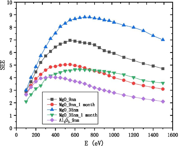
Variação de SEE de 9 nm-Al 2 O 3 9 nm-MgO e 35 nm-MgO com a energia do elétron incidente, e o resultado medido após 1 mês de deliquescência de ar da amostra
Sabe-se que os produtos finais de MgO deliquescente são principalmente Mg 2 (OH) 2 CO 3 e MgCO 3 , de modo que o conteúdo da concentração do átomo de C em diferentes profundidades do material pode refletir a profundidade deliquescente de MgO. A superfície é gravada por sputtering de feixe de íons de Ar e analisada por espectroscopia de fotoelétrons de raios-X (XPS). Os dois são executados alternadamente. A profundidade de corrosão é controlada pelo controle do tempo de corrosão, e as mudanças percentuais da concentração atômica relativa dos elementos C e Mg são obtidas por XPS. Quando o XPS não pode medir a porcentagem de concentração relativa do elemento C, a profundidade de corrosão neste momento é a profundidade deliquescente de MgO. O método acima mostra que a profundidade deliquescente de MgO é de cerca de 3,8 nm e 1 nm de Al 2 O 3 pode proteger o MgO de deliquescent.
Para medir o nível SEE dos materiais, muitos laboratórios em todo o mundo construíram seus próprios dispositivos de medição dedicados, incluindo Stanford Linear Accelerator Center [14], a University of Utah [22], Princeton University [23]; ONERA / DESP [24]; Universidade de Ciência e Tecnologia da China, Xi'an Jiaotong University, 504 Institute of Aerospace, China Spallation Neutron Source, University Of Electronic Science and Technology Of China, etc. Projetamos um sistema esférico para testar o nível SEE de materiais para garantir que coleção completa de elétrons secundários e ajudam a melhorar a precisão dos resultados da medição. E, recomendamos o uso de elétrons secundários de baixa energia em vez de feixes de elétrons de baixa energia para neutralização para medir o SEE de materiais isolantes, como MgO e Al 2 O 3 , evita as desvantagens da dose de neutralização e do tempo de neutralização [24, 25], este método é conveniente e de baixo custo.
Projetamos a camada de emissão do multiplicador de elétrons com a ideia de construir uma casa e obtivemos bons resultados. Comparamos o valor SEE sob a energia do elétron incidente dos vizinhos e usamos isso como um padrão para dividir o material em uma região de baixa energia, uma região de média energia e uma região de alta energia. Isso é diferente do campo de supressão de micro-descarga [14]. Verifica-se que a região de energia média pode eliminar a interferência da energia do elétron incidente no valor SEE. Portanto, a região de energia média é selecionada como o padrão para medir o nível SEE do material, e Al 2 O 3 , MgO, MgO / Al 2 O 3 , Al 2 O 3 / MgO são estudados para obter a fórmula empírica.
O principal modelo físico SEE proposto atualmente é o modelo de Dionne [26, 27]. O modelo de camada dupla proposto [28] é posteriormente revisado e não é adequado para os dados experimentais atuais. Portanto, sugerimos usar o conceito de camada de transição para explicar os materiais multicamadas, o que pode dar uma boa explicação das características do material do projeto.
Nossos experimentos e cálculos descobriram que depois de cultivar Al 2 O 3 e, em seguida, crescendo MgO, o nível SEE saturado de MgO pode ser revelado quando este filme é mais fino do que o filme de MgO. Isso resolve o problema de que o filme de MgO é muito espesso e a camada condutora não pode complementar a carga da camada de emissão. E descobrimos que depois de cultivar MgO e então cultivar Al 2 O 3 , Al 2 O 3 acima de 3 nm não mostra mais o nível SEE de MgO; o 1 nm Al 2 O 3 pode resistir aos danos do ambiente externo ao MgO, e manter o nível SEE de MgO por muito tempo; o 0,3 nm Al 2 O 3 pode aumentar o nível SEE saturado de MgO. Portanto, propomos que o processo de preparação da nova camada de emissão é fazer crescer uma camada principal de MgO de 9 nm no Al de 2 nm 2 O 3 camada tampão e, em seguida, cresça 1 nm de Al 2 O 3 camada protetora ou 0,3 nm Al 2 O 3 camada de realce sobre ele, que pode resolver o problema das deficiências de MgO da camada de emissão nos multiplicadores de elétrons. Melhoramos muito o ganho da placa de microcanais, aumentando esse novo tipo de camada de emissão no microcanal da placa de microcanais (uma espécie de multiplicador de elétrons). A espessura do projeto desta nova camada de emissão é de grande importância para melhorar o ganho e a estabilidade do multiplicador de elétrons.
Experimental e Métodos
A camada de emissão usando deposição de camada atômica
A deposição da camada atômica (ALD) é um tipo de tecnologia em que o gás precursor e o gás de reação entram alternadamente na superfície basal a uma taxa controlada, adsorção física ou química na superfície ou ocorre reação saturada na superfície, o material é depositado camada por camada na forma de um único filme de átomo na superfície. ALD pode produzir filme contínuo sem pino-microcanal, tem excelente cobertura e pode controlar a espessura e composição do filme atômico. Portanto, escolhemos ALD como um método de preparação importante para estudar a espessura da camada de emissão.
A seguir está a equação de reação química do uso de ALD para cultivar Al 2 O 3 :
$$ \ begin {alinhados} {\ text {A}} &:{\ text {Substrato}} - {\ text {OH}} ^ {*} + {\ text {Al}} \ left ({{\ text {CH}} _ {3}} \ right) _ {3} \ to {\ text {Substrato}} - {\ text {O}} - {\ text {Al}} \ left ({{\ text {CH }} _ {3}} \ right) _ {2} ^ {*} + {\ text {CH}} _ {4} \ uparrow \\ {\ text {B}} &:{\ text {Substrato}} - {\ text {O}} - {\ text {Al}} \ left ({{\ text {CH}} _ {3}} \ right) _ {2} ^ {*} + 2 {\ text {H }} _ {2} {\ text {O}} \ to {\ text {Substrato}} - {\ text {O}} - {\ text {Al}} \ left ({{\ text {OH}}} \ right) _ {2} ^ {*} + 2 {\ text {CH}} _ {4} \ uparrow \\ {\ text {C}} &:{\ text {Al}} - {\ text {OH }} ^ {*} + {\ text {Al}} \ left ({{\ text {CH}} _ {3}} \ right) _ {3} \ to {\ text {Al}} - {\ text {O}} - {\ text {Al}} \ left ({{\ text {CH}} _ {3}} \ right) _ {2} ^ {*} + {\ text {CH}} _ {4 } \ uparrow \\ {\ text {D}} &:{\ text {Al}} - {\ text {CH}} _ {3} ^ {*} + {\ text {H}} _ {2} { \ text {O}} \ to {\ text {Al}} - {\ text {OH}} ^ {*} + 2 {\ text {CH}} _ {4} \ uparrow \\ \ end {alinhados} $ $
Como mostra a equação de A e B ou C e D, a superfície basal foi originalmente coberta com –OH, a reação química de –OH e Al (CH 3 ) 3 (TMA) formou o novo –CH 3 superfície e liberou CH 4 (subproduto). O novo –CH 3 superfície exposta ao vapor de água, sua reação gerou a nova superfície –OH e liberou CH 4 novamente. A temperatura da reação é de 200 ° C. O tempo e a ordem de crescimento de uma camada de Al 2 O 3 átomo, conforme mostrado na Fig. 2:
$$ {\ text {TMA / N}} _ {2} {\ text {/ H}} _ {2} {\ text {O / N}} _ {2} =0,1 \ sim 1 {\ text {s }} / 5 \ sim 45 {\ text {s}} / 0,1 \ sim 1 {\ text {s}} / 5 \ sim 45 {\ text {s}} {.} $$
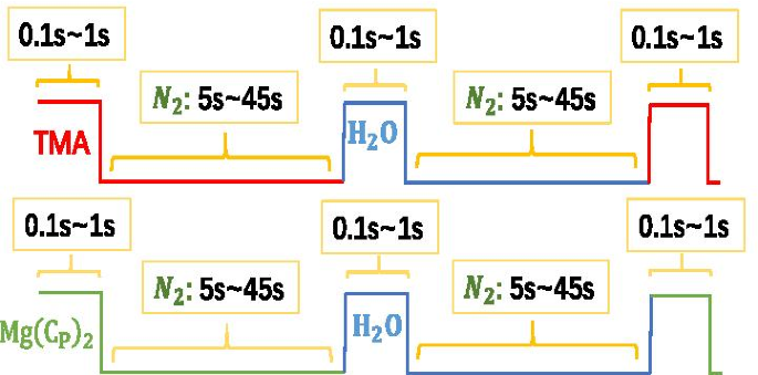
Diagrama esquemático do processo de crescimento de Al 2 O 3 e MgO
A seguir está a equação de reação química do uso de ALD para cultivar MgO:
$$ \ begin {alinhados} {\ text {E}} &:{\ text {Substrato}} - {\ text {OH}} ^ {*} + {\ text {Mg}} \ left ({{\ text {C}} _ {5} {\ text {H}} _ {5}} \ right) _ {2} \ to {\ text {Substrato}} - {\ text {O}} - {\ text {MgC }} _ {5} {\ text {H}} _ {5} ^ {*} + {\ text {C}} _ {5} {\ text {H}} _ {6} \ uparrow \\ {\ text {F}} &:{\ text {Substrate}} - {\ text {O}} - {\ text {MgC}} _ {5} {\ text {H}} _ {5} ^ {*} + {\ text {H}} _ {2} {\ text {O}} \ to {\ text {Substrato}} - {\ text {OH}} ^ {*} + {\ text {C}} _ {5 } {\ text {H}} _ {6} \ uparrow \\ {\ text {G}} &:{\ text {Mg}} - {\ text {OH}} ^ {*} + {\ text {Mg }} \ left ({{\ text {C}} _ {5} {\ text {H}} _ {5}} \ right) _ {2} \ to {\ text {Mg}} - {\ text { O}} - {\ text {MgC}} _ {5} {\ text {H}} _ {5} ^ {*} + {\ text {C}} _ {5} {\ text {H}} _ {6} \ uparrow \\ {\ text {H}} &:{\ text {Mg}} - {\ text {C}} _ {5} {\ text {H}} _ {5} ^ {*} + {\ text {H}} _ {2} {\ text {O}} \ to {\ text {Mg}} - {\ text {OH}} ^ {*} + {\ text {C}} _ { 5} {\ text {H}} _ {6} \ uparrow \\ \ end {alinhado} $$
Como a equação de E e F ou G e H mostrado, a superfície basal foi originalmente coberta com \ (- {\ text {OH}} \), A reação química de \ (- {\ text {OH}} \) e \ ({\ text {Mg}} \ left ({{\ text {C}} _ {5} {\ text {H}} _ {5}} \ right) _ {2} \) (\ ({\ texto {Mg}} \ left ({{\ text {C}} _ {{\ text {P}}}} \ right) _ {2} \)) formou o novo \ (- {\ text {C}} _ {5} {\ text {H}} _ {5} \) superfície, e liberado \ ({\ text {C}} _ {5} {\ text {H}} _ {6} \) (subproduto) . A nova superfície \ (- {\ text {C}} _ {5} {\ text {H}} _ {5} \) exposta ao vapor d'água, sua reação gerou o novo \ (- {\ text {OH}} \) superfície e liberado \ ({\ text {C}} _ {5} {\ text {H}} _ {6} \) novamente.
Aquecemos \ ({\ text {Mg}} \ left ({{\ text {C}} _ {{\ text {P}}}} \ right) _ {2} \) a 60 ° C para transformá-lo em pó. A temperatura da câmara de reação é de 200 ° C. O tempo e a ordem de crescimento de uma camada de átomo de MgO, conforme mostrado na Fig. 2:
$$ {\ text {Mg}} \ left ({{\ text {Cp}}} \ right) _ {2} {\ text {/ N}} _ {2} {\ text {/ H}} _ { 2} {\ text {O / N}} _ {2} =0,1 \ sim 1 {\ text {s}} / 5 \ sim 45 {\ text {s}} / 0,1 \ sim 1 {\ text {s} } / 5 \ sim 45 {\ text {s}} {.} $$
O projeto da camada de emissão
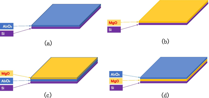
As amostras são preparadas de quatro maneiras, conforme mostrado na Fig. 3:crescer diferentes espessuras de \ ({\ text {Al}} _ {2} {\ text {O}} _ {3} \) em pastilha de Si; cultivar diferentes espessuras de MgO na pastilha de Si; aumente diferentes espessuras de \ ({\ text {Al}} _ {2} {\ text {O}} _ {3} \) na pastilha de Si e então cresça espessuras fixas de MgO; cresça uma espessura fixa de MgO no wafer de Si e, em seguida, cresça uma espessura diferente de \ ({\ text {Al}} _ {2} {\ text {O}} _ {3} \). Nós desenvolvemos diferentes espessuras de \ ({\ text {Al}} _ {2} {\ text {O}} _ {3} \) em wafer de Si (1 nm, 3 nm, 7 nm, 9 nm, 30 nm , 50 nm). Temos crescido diferentes espessuras de MgO em pastilha de Si (1 nm, 3 nm, 5 nm, 9 nm, 15 nm, 20 nm, 35 nm). Crescemos diferentes espessuras de \ ({\ text {Al}} _ {2} {\ text {O}} _ {3} \) na bolacha de Si (0,6 nm, 1 nm, 3 nm, 30 nm) e depois crescemos espessuras fixas de MgO (9 nm). Nós crescemos uma espessura fixa de MgO no wafer de Si (35 nm) e, em seguida, crescemos uma espessura diferente de \ ({\ text {Al}} _ {2} {\ text {O} } _ {3} \) (0,3 nm, 0,6 nm, 1 nm, 3 nm, 5 nm, 7 nm, 10 nm, 20 nm).
Pesquisa sobre a relação entre a espessura do filme e SEE, projetando o experimento da camada de emissão
O novo método de teste para SEE
Usamos o método do coletor para medir como mostrado na Fig. 4:primeiro conecte o estágio de amostra ao coletor, a corrente medida pelo picoamperímetro é a corrente de elétron incidente, denotada como \ (I _ {{\ text {p}}} \ ); sob as mesmas condições de incidente, desconecte a amostra e o coletor, neste momento a corrente medida no coletor é a corrente de elétron secundária, denotada como \ (I _ {{\ text {s}}} \).
$$ {\ text {VER}} =\ frac {{I _ {{\ text {s}}}}} {{I _ {{\ text {p}}}}} $$
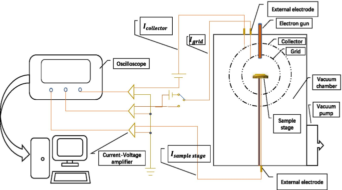
Diagrama esquemático do sistema de eficiência de emissão de elétrons secundários
Projetamos o dispositivo em uma estrutura de formato global para garantir a coleção completa de elétrons secundários e ajudar a melhorar a precisão dos resultados da medição.
Quando o material isolante é bombardeado por elétrons incidentes, a superfície do material emite elétrons secundários e acumula cargas positivas devido à perda de elétrons. A carga positiva aumenta o potencial. Porque os elétrons secundários são gerados a poucos nanômetros da superfície do material e têm baixa energia (~ eV). Os elétrons secundários são muito suscetíveis ao potencial positivo. O potencial positivo afetará o próximo processo de emissão de elétrons secundários, levando a um declínio no rendimento de elétrons secundários.
A fim de eliminar o efeito do acúmulo de carga no resultado da medição do SEE da amostra isolante e medir com precisão o SEE da amostra isolante, o método tradicional usa diretamente um feixe de elétrons de baixa energia para irradiar a amostra isolante, e o positivo carga na superfície da amostra é neutralizada pelo elétron de baixa energia. O método tradicional tem duas desvantagens. Primeiro, ele precisa calcular com precisão a dose de neutralização, é fácil ter carga positiva na superfície da amostra devido à dose de neutralização insuficiente, ou carga negativa na superfície da amostra devido à neutralização excessiva; segundo, ele precisa ser equipado com outro canhão de elétrons de baixa energia [24, 25].
Propomos o uso de elétrons secundários de baixa energia em vez de feixe de elétrons de baixa energia para neutralização, o que supera as deficiências dos métodos tradicionais e obtém elétrons secundários precisos, como mostrado na Fig. 5 [29]. Colocamos a amostra de isolamento a ser testada em metade do estágio de amostra e deixamos a outra metade vazia. A mesa de amostra é feita de aço inoxidável 304 e o potencial elétrico é 0 V.
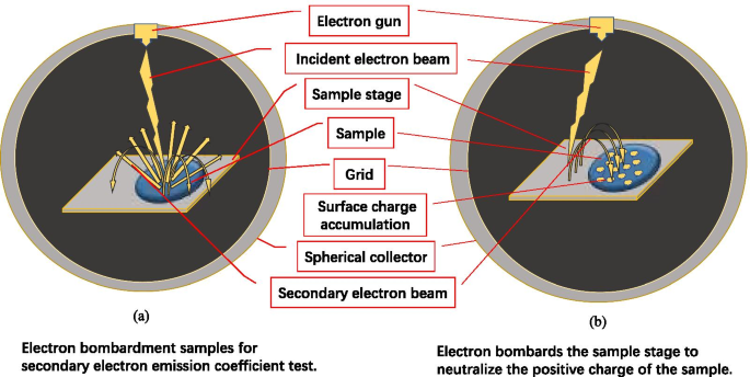
Diagrama esquemático do novo método de teste para o coeficiente de emissão de elétrons secundários do material
Ao testar uma amostra isolante, os elétrons gerados pelo canhão de elétrons bombardeiam a superfície da amostra isolante como mostrado na Fig. 5a, resultando em uma área de carga positiva como mostrado na Fig. 5b. Ao neutralizar a carga superficial da amostra isolante, a área meio vazia do estágio de amostra é bombardeada ajustando o ângulo do canhão de elétrons para fazer o estágio de amostra emitir elétrons secundários como mostrado na Fig. 5b.
Devido à atração mútua de cargas positivas e elétrons, elétrons secundários são atraídos para a superfície da amostra para neutralização de carga. À medida que a carga positiva diminui, menos elétrons são atraídos. Quando a carga positiva na superfície da amostra é neutralizada, a superfície da amostra isolante retorna ao seu estado original. Como não há carga positiva, ele não continuará a atrair os elétrons secundários de baixa energia gerados pelo estágio de amostra, portanto, não haverá neutralização excessiva que faça com que a superfície da amostra seja carregada negativamente.
O canhão de elétrons que usamos bombardeia a superfície da amostra na mesma posição todas as vezes e, em seguida, desvia o mesmo ângulo para bombardear a mesma posição no estágio de amostra, conforme mostrado na Fig. 6. Devido ao processo de teste SEE de longo prazo, a posição no estágio de amostra bombardeado pelo canhão de elétrons por um longo tempo tornou-se um ponto negro, como mostrado na Fig. 6.
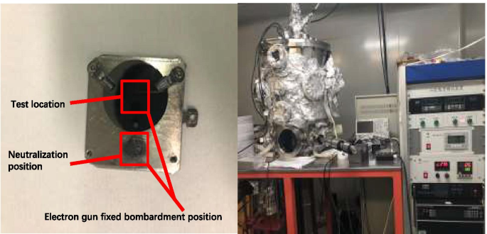
Fotografias da amostra, o estágio da amostra e o equipamento de teste de coeficiente de emissão de elétrons secundários
Resultado e discussão
VEJA Zoneamento e análise
Comparamos o valor SEE sob a energia dos elétrons incidentes adjacentes para descrever a mudança de SEE com a energia dos elétrons incidentes e definimos como
$$ R _ {{{\ text {VER}}}} =\ frac {{{\ text {VER}} \ left ({x + b} \ right)}} {{{\ text {VER}} \ left ({x} \ right)}} $$
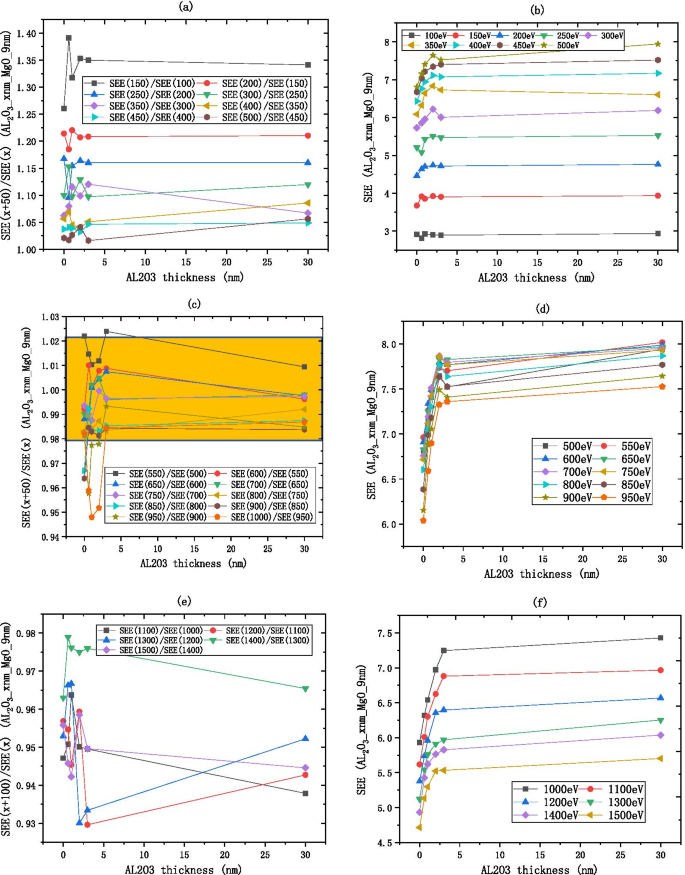
e o SEE do material é dividido em três áreas pelo tamanho do valor \ (R _ {{{\ text {SEE}}}} \), ou seja, a região de baixa energia do elétron incidente (\ (R _ {{{ \ text {SEE}}}} \ ge 1.02 \)), a região de energia média do elétron incidente (\ (0.98 \ le R _ {{{\ text {SEE}}}} <1.02 \)) e a alta energia região do elétron incidente (\ ({\ text {R}} _ {{{\ text {SEE}}}} \ ge 0.98 \)). A faixa de energia do elétron incidente do material que usamos para testar SEE é (100 eV, 1500 eV), x representa a energia do elétron incidente, e b representa o comprimento do passo da energia do elétron incidente no teste SEE.
\ ({\ text {Al}} _ {2} {\ text {O}} _ {3} \) SEE basicamente permanece inalterado após 7 nm, como mostrado na Fig. 7. Como mostrado na Fig. 7a, b, o região de baixa energia de \ ({\ text {Al}} _ {2} {\ text {O}} _ {3} \) está entre 100 e 250 eV, o \ (R _ {{{\ text {VER}} }} \) diminui de 1,25 para 1,02, indicando que conforme a energia do elétron incidente aumenta, o SEE aumenta e finalmente se estabiliza. Conforme mostrado na Fig. 7c, d, a região de energia média de \ ({\ text {Al}} _ {2} {\ text {O}} _ {3} \) está entre 250 e 500 eV, o \ ( R _ {{{\ text {SEE}}}} \) é considerado constante dentro do intervalo de [0,98, 1,02], ou seja, o \ (R _ {{{\ text {SEE}}}} \) é aproximadamente igual para 1, indicando que o SEE está basicamente inalterado à medida que a energia do elétron incidente aumenta. Conforme mostrado na Fig. 7e, f, a região de alta energia de \ ({\ text {Al}} _ {2} {\ text {O}} _ {3} \) está entre 500 e 1500 eV, para cada aumento de 200 eV de energia elétrica incidente, o SEE diminui cerca de 0,9 vezes.
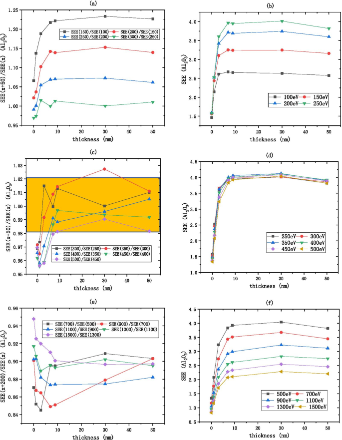
Depois de dividir a energia do elétron incidente por \ (R _ {{{\ text {VER}}}} =\ frac {{\ text {VER (x + b)}}} {{\ text {VER (x)}}} \) conforme mostrado no a , c , e a mudança de Al 2 O 3 (no wafer de silício, cresça xnm-Al 2 O 3 ) VER com espessura conforme mostrado no b , d , f
O MgO SEE basicamente permanece inalterado após 20 nm, conforme mostrado na Fig. 9. Conforme mostrado na Fig. 8a, b, a região de baixa energia do MgO está entre 100 e 500 eV, o \ (R _ {{{\ text {SEE} }}} \) diminui de 1,3 para 1, indicando que conforme a energia do elétron incidente aumenta, o SEE aumenta e finalmente se estabiliza. Conforme mostrado na Fig. 8c, d, a região de energia média do MgO está entre 500 e 1000 eV, o \ (R _ {{{\ text {SEE}}}} \) é considerado constante dentro do intervalo de [0,98, 1,02 ], ou seja, o \ (R _ {{{\ text {SEE}}}} \) é aproximadamente igual a 1, indicando que o SEE é basicamente inalterado à medida que a energia do elétron incidente aumenta. Conforme mostrado na Fig. 8e, f, a região de alta energia do MgO está entre 1000 e 1500 eV, para cada aumento de 100 eV da energia do elétron incidente, o SEE diminui cerca de 0,94 vezes.
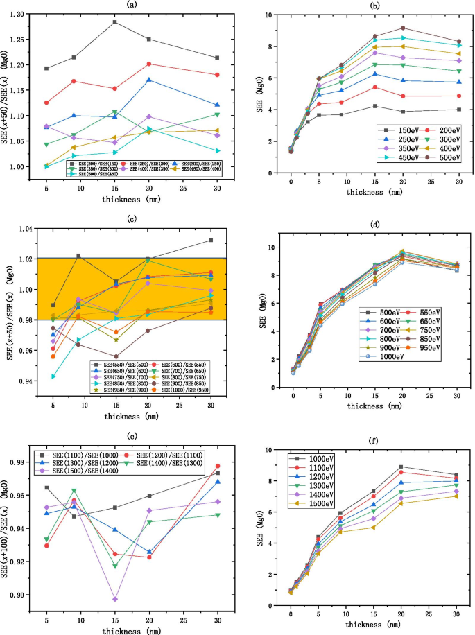
Depois de dividir a energia do elétron incidente por \ (R _ {{{\ text {VER}}}} =\ frac {{\ text {VER (x + b)}}} {{\ text {VER (x)}}} \) conforme mostrado no a , c , e a mudança de MgO (no wafer de silício, cresça xnm-MgO) VEJA com a espessura conforme mostrado no b , d , f
Conforme mostrado na Fig. 9, O SEE de \ ({\ text {Al}} _ {2} {\ text {O}} _ {3} \) / MgO e MgO têm partição de energia elétrica incidente semelhante, o SEE de \ ({\ text {Al}} _ {2} {\ text {O}} _ {3} \) / MgO basicamente permanece inalterado após 3 nm. Conforme mostrado na Fig. 9a, b, a região de baixa energia de \ ({\ text {Al}} _ {2} {\ text {O}} _ {3} \) / MgO está entre 100 e 450 eV, o \ (R _ {{{\ text {SEE}}}} \) diminui de 1,4 para 1,05, indicando que conforme a energia do elétron incidente aumenta, o SEE aumenta e finalmente se estabiliza. Conforme mostrado na Fig. 9c, d, a região de energia média de \ ({\ text {Al}} _ {2} {\ text {O}} _ {3} \) / MgO está entre 500 e 1000 eV, o \ (R _ {{{\ text {SEE}}}} \) é considerado constante dentro do intervalo de [0,98, 1,02], ou seja, o \ (R _ {{{\ text {SEE}}}} \) é aproximadamente igual a 1, indicando que o SEE é basicamente inalterado à medida que a energia do elétron incidente aumenta. Conforme mostrado na Fig. 9e, f, a região de alta energia de \ ({\ text {Al}} _ {2} {\ text {O}} _ {3} \) / MgO está entre 1000 e 1500 eV, para a cada aumento de 100 eV de energia elétrica incidente, o SEE diminui cerca de 0,95 vezes. Como o SEE de \ ({\ text {Al}} _ {2} {\ text {O}} _ {3} \) / MgO é estável na região de energia média, a energia do elétron incidente pode ser excluída como uma variável fator.
Depois de dividir a energia do elétron incidente por \ (R _ {{{\ text {VER}}}} =\ frac {{\ text {VER (x + b)}}} {{\ text {VER (x)}}} \) conforme mostrado no a , c , e a mudança de Al 2 O 3 / MgO (no wafer de silício, crescer xnm-Al 2 O 3 e, em seguida, cresça 9 nm-MgO) VEJA com a espessura mostrada em b , d , f
Conforme mostrado na Fig. 10, O SEE de MgO / \ ({\ text {Al}} _ {2} {\ text {O}} _ {3} \) e \ ({\ text {Al}} _ { 2} {\ text {O}} _ {3} \) têm partição de energia elétrica incidente semelhante, a SEE de MgO / \ ({\ text {Al}} _ {2} {\ text {O}} _ {3 } \) basicamente permanece inalterado após 3 nm. Conforme mostrado na Fig. 10a, b, a região de baixa energia de MgO / \ ({\ text {Al}} _ {2} {\ text {O}} _ {3} \) está entre 100 e 300 eV, o \ (R _ {{{\ text {SEE}}}} \) diminui de 1,8 para 1, indicando que conforme a energia do elétron incidente aumenta, o SEE aumenta e finalmente se estabiliza. Conforme mostrado na Fig. 10c, d, a região de energia média de MgO / \ ({\ text {Al}} _ {2} {\ text {O}} _ {3} \) está entre 300 e 500 eV, o \ (R _ {{{\ text {SEE}}}} \) é considerado constante no intervalo de [0,98, 1,02], quando \ ({\ text {Al}} _ {2} {\ text {O}} _ {3} \) é fino, \ (R _ {{{\ text {SEE}}}} \) desvia de 1, e a diferença em SEE sob diferentes energias de elétrons incidentes é óbvia; quando \ ({\ text {Al}} _ {2} {\ text {O}} _ {3} \) é grosso, \ (R _ {{{\ text {SEE}}}} \) é próximo a 1 , e a diferença não é óbvia. Conforme mostrado na Fig. 10e, f, a região de alta energia de MgO / \ ({\ text {Al}} _ {2} {\ text {O}} _ {3} \) está entre 500 e 1500 eV, quando \ ({\ text {Al}} _ {2} {\ text {O}} _ {3} \) é fino, \ (R _ {{{\ text {SEE}}}} \) é próximo de 1, e a diferença em SEE sob diferentes energias de elétrons incidentes não é óbvia; quando \ ({\ text {Al}} _ {2} {\ text {O}} _ {3} \) é grosso, \ (R _ {{{\ text {SEE}}}} \) desvia de 1, e a diferença é óbvia; para cada aumento de 200 eV de energia elétrica incidente, o SEE diminui cerca de 0,9 vezes.
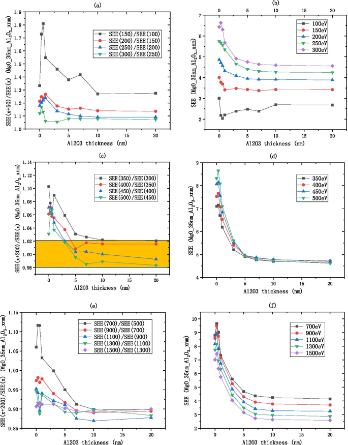
Depois de dividir a energia do elétron incidente por \ (R _ {{{\ text {VER}}}} =\ frac {{\ text {VER (x + b)}}} {{\ text {VER (x)}}} \) conforme mostrado em a, c, e , a mudança de MgO / Al 2 O 3 (no wafer de silício, cresça 35 nm-MgO e, em seguida, cresça xnm-Al 2 O 3 ) VER com espessura conforme mostrado no b , d, f
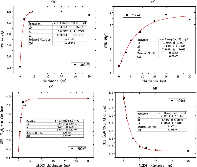
Como o \ ({\ text {Al}} _ {2} {\ text {O}} _ {3} \) SEE é estável na região de energia média, a energia do elétron incidente pode ser excluída como um fator variável. Escolhemos a energia elétrica incidente média 300 eV como o padrão para medir o nível SEE de \ ({\ text {Al}} _ {2} {\ text {O}} _ {3} \), a fórmula empírica para o espessura de \ ({\ text {Al}} _ {2} {\ text {O}} _ {3} \) e o melhor SEE é obtido pelo ajuste conforme mostrado na Fig. 11a (Tabela 1).
$$ {\ text {B}} \ _ {\ text {VER}} _ {{{\ text {Al}} _ {2} {\ text {O}} _ {3}}} =3,99 - 2,5 { *} e ^ {{- \ frac {{{\ text {espessura}}}} {1,73}}} $$ (1)
Relationship between the material's best secondary electron emission coefficient and film thickness, a shows the information of Al2 O3 (on the silicon wafer, grow xnm-Al2 O3 ), b shows the information of MgO (on the silicon wafer, grow xnm-MgO), c shows the information of Al2 O3 /MgO (on the silicon wafer, grow xnm-Al2 O3 , and then grow 9 nm-MgO), and d shows the information of MgO/Al2 O3 (on the silicon wafer, grow 35 nm-MgO, and then grow xnm-Al2 O3 )
Because the MgO SEE is stable in the medium energy region, the incident electron energy can be excluded as a variable factor. We choose the medium incident electron energy 700 eV as the standard to measure the SEE level of MgO, the empirical formula for the thickness of alumina material and the best SEE is obtained by fitting as shown in Fig. 11b.
$${\text{B}}\_{\text{SEE}}_{{{\text{MgO}}}} =9.56 - 8.64*e^{{ - \frac{{{\text{thickness}}}}{7.39}}}$$ (2)
Because the SEE of \({\text{Al}}_{2} {\text{O}}_{3} /{\text{MgO}}\) is stable in the medium energy region, the incident electron energy can be excluded as a variable factor. We choose the medium incident electron energy 700 eV as the standard to measure the SEE level of \({\text{Al}}_{2} {\text{O}}_{3}\)/MgO, the empirical formula for the thickness of alumina material and the best SEE is obtained by fitting as shown in Fig. 11c.
$${\text{B}}\_{\text{SEE}}_{{{\text{Al}}_{2} {\text{O}}_{3} /{\text{MgO}}}} =7.94 - 1.21\,*\,e^{{ - \frac{{{\text{thickness}}}}{1.03}}}$$ (3)
Because the SEE of MgO/\({\text{Al}}_{2} {\text{O}}_{3}\) is stable in the medium energy region, the incident electron energy can be excluded as a variable factor. We choose the medium incident electron energy 450 eV as the standard to measure the SEE level of MgO/\({\text{Al}}_{2} {\text{O}}_{3}\), the empirical formula for the thickness of alumina material and the best SEE is obtained by fitting as shown in Fig. 11d.
$${\text{B}}\_{\text{SEE}}_{{{\text{MgO}}/{\text{Al}}_{2} {\text{O}}_{3} }} =4.69 + 3.64\,*\,e^{{ - \frac{{{\text{thickness}}}}{2.11}}}$$ (4) $$\frac{{{\text{B}}\_{\text{SEE}}_{{{\text{MgO}}}} \left( 9 \right)}}{{{\text{B}}\_{\text{SEE}}_{{{\text{Al}}_{2} {\text{O}}_{3} }} \left( {30} \right)}} =\frac{{9.56 - 8.64\,*\,e^{{ - \frac{9}{7.39}}} }}{{3.99 - 2.5\,*\,e^{{ - \frac{30}{{1.73}}}} }} \approx 1.755$$
According to formulas 1 and 2, the SEE level of 9 nm MgO is 1.755 times higher than that of 30 nm \({\text{Al}}_{2} {\text{O}}_{3}\).
$$\begin{aligned} \frac{{{\text{B}}\_{\text{SEE}}_{{{\text{Al}}_{2} {\text{O}}_{3} /{\text{MgO}}}} \left( 3 \right)}}{{{\text{B}}\_{\text{SEE}}_{{{\text{Al}}_{2} {\text{O}}_{3} }} \left( {30} \right)}} &=\frac{{7.94 - 1.21\,*\,e^{{ - \frac{3}{{1.03}}}} }}{{3.99 - 2.5\,*\,e^{{ - \frac{{30}}{{1.73}}}} }} \approx 1.973 \\ \frac{{{\text{B}}\_{\text{SEE}}_{{{\text{Al}}_{2} {\text{O}}_{3} /{\text{MgO}}}} \left( 3 \right)}}{{{\text{B}}_{{{\text{SEE}}\,{\text{MgO}}}} \left( 9 \right)}} &=\frac{{7.94 - 1.21\,*\,e^{{ - \frac{3}{{1.03}}}} }}{{9.56 - 8.64\,*\,e^{{ - \frac{9}{{7.39}}}} }} \approx 1.124 \\ \end{aligned}$$
We deposit 0–30 nm \({\text{Al}}_{2} {\text{O}}_{3}\) and redeposit 9 nm MgO on the Si wafer as the film, as shown in Fig. 12a. formulas 1 and 3 show that the SEE level of 9 nm MgO grown on 3 nm \({\text{Al}}_{2} {\text{O}}_{3}\) is 1.973 times higher than that of \({\text{Al}}_{2} {\text{O}}_{3}\). formulas 2 and 3 show that the SEE level of 9 nm MgO grown on 3 nm \({\text{Al}}_{2} {\text{O}}_{3}\) is 1.124 times higher than that of 9 nm MgO.
$$\frac{{{\text{B}}\_{\text{SEE}}_{{{\text{MgO}}/{\text{Al}}_{2} {\text{O}}_{3} }} }}{{{\text{B}}\_{\text{SEE}}_{{{\text{Al}}_{2} {\text{O}}_{3} }} }} =\frac{{4.69 + 3.64\,*\,e^{{ - \frac{1}{2.11}}} }}{{3.99 - 2.5\,*\,e^{{ - \frac{30}{{1.73}}}} }} \approx 1.743$$

Change of secondary electron emission coefficient with different incident electron energy, a shows the information of Al2 O3 /MgO (on the silicon wafer, grow xnm-Al2 O3 , and then grow 9 nm-MgO), b shows the information of MgO/Al2 O3 and deliquescent MgO/Al2 O3 (on the silicon wafer, grow 35 nm-MgO, and then grow 1 nm-Al2 O3 ), c shows the information of MgO/Al2 O3 (on the silicon wafer, grow 35 nm-MgO, and then grow 0.3 nm-Al2 O3 ), and d shows the information of Al2 O3 /MgO (on the silicon wafer, grow 3 nm-Al2 O3 , and then grow 5 nm-MgO)
The SEE level of MgO after deliquescent drops significantly as shown in Fig. 1. Then, we deposit 35 nm MgO and redeposit 1 nm \({\text{Al}}_{2} {\text{O}}_{3}\) on the Si wafer as the film. We found the SEE of this film exposed to the air 7 months is close to the SEE without exposed to the air as shown in Fig. 12b. Formulas 1 and 3 show that the SEE level of 1 nm \({\text{Al}}_{2} {\text{O}}_{3}\) grown on MgO is 1.743 times higher than the SEE of \({\text{Al}}_{2} {\text{O}}_{3}\) and can be long-term maintain a high SEE level (no obvious deliquescence in 7 months).
$$\begin{aligned} \frac{{{\text{B}}\_{\text{SEE}}_{{{\text{MgO}}/{\text{Al}}_{2} {\text{O}}_{3} }} \left( {0.3} \right)}}{{{\text{B}}\_{\text{SEE}}_{{{\text{Al}}_{2} {\text{O}}_{3} }} \left( {30} \right)}} &=\frac{{4.69 + 3.64\,*\,e^{{ - \frac{0.3}{{2.11}}}} }}{{3.99 - 2.5\,*\,e^{{ - \frac{30}{{1.73}}}} }} \approx 1.967, \\ \frac{{{\text{B}}\_{\text{SEE}}_{{{\text{MgO}}/{\text{Al}}_{2} {\text{O}}_{3} }} \left( {0.3} \right)}}{{{\text{B}}\_{\text{SEE}}_{{{\text{MgO}}}} \left( 9 \right)}} &=\frac{{4.69 + 3.64\,*\,e^{{ - \frac{0.3}{{2.11}}}} }}{{9.56 - 8.64\,*\,e^{{ - \frac{9}{7.39}}} }} \approx 1.12 \\ \end{aligned}$$
We deposited 35 nm MgO on the Si wafer and re-deposited 0.3 nm \({\text{Al}}_{2} {\text{O}}_{3}\) as a thin film as shown in Fig. 12c. It can be seen from formulas 1, 2 and 4 that the SEE level of 0.3 nm \({\text{Al}}_{2} {\text{O}}_{3}\) grown on MgO is 1.967 times higher than that of \({\text{Al}}_{2} {\text{O}}_{3}\) and 1.12 times higher than that of MgO;
The emission layer of the electron multiplier pursues thinner and higher SEE level, so we sacrificed some SEE level to make the film thinner. We deposited 3 nm \({\text{Al}}_{2} {\text{O}}_{3}\) on the Si wafer and re-deposited 5 nm MgO as a thin film as shown in Fig. 12d.
We propose to grow 2–3 nm \({\text{Al}}_{2} {\text{O}}_{3}\) as a buffer layer, grow 5–9 nm MgO as the main layer, and grow 0.3 nm \({\text{Al}}_{2} {\text{O}}_{3}\) as an enhancement layer or 1 nm \({\text{Al}}_{2} {\text{O}}_{3}\) as a protective layer as the \({\text{Al}}_{2} {\text{O}}_{3}\)/MgO/\({\text{Al}}_{2} {\text{O}}_{3}\) emissive layer of electron multipliers as shown in Fig. 13. SEE level of \({\text{Al}}_{2} {\text{O}}_{3}\)/MgO/\({\text{Al}}_{2} {\text{O}}_{3}\) emission layer (\({\text{Al}}_{2} {\text{O}}_{3}\)/MgO/\({\text{Al}}_{2} {\text{O}}_{3}\) = 3 nm/9 nm/0.3 nm) is shown in Fig. 12a. And, we tested a traditional microchannel plate with good gain and then grew \({\text{Al}}_{2} {\text{O}}_{3}\)/MgO/\({\text{Al}}_{2} {\text{O}}_{3}\) emission layer on microchannel wall of microchannel plate, and the gain result obtained by the test was significantly improved. Then, another piece of the first convention microchannel plate with close gain is grown with \({\text{Al}}_{2} {\text{O}}_{3}\) emission layer. Compared with the gain results obtained by the test, the \({\text{Al}}_{2} {\text{O}}_{3}\)/MgO/\({\text{Al}}_{2} {\text{O}}_{3}\) emission layer structure is more superior as shown in Fig. 14.

Schematic diagram of sandwich structure (Al2 O3 /MgO/Al2 O3 )

Relationship between the voltage and gain of the three microchannel plates (conventional microchannel plate, microchannel plate for growing Al2 O3 emission layer, microchannel plate for growing Al2 O3 /MgO/Al2 O3 emission layer)
XPS Characterization and Transition Layer Concept
SEE data usually uses Dionne model for fitting analysis [26, 27]. The current double-layer model based on Dionne model does not consider the existence of a transition layer between the two materials. Through the design of the emission layer structure this time, the SEE difference between \({\text{Al}}_{2} {\text{O}}_{3}\)/MgO and \({\text{Si}}\)/MgO can be clearly observed. Under the same SEE level, MgO exhibits a very large thickness difference. Sample (0.3 nm \({\text{Al}}_{2} {\text{O}}_{3}\) grown on MgO) can get a higher SEE than MgO. Sample (1 nm \({\text{Al}}_{2} {\text{O}}_{3}\) grown on MgO) maintain a high SEE level. The current double-layer model [28] can no longer explain the above phenomenon, so we put forward the concept of transition layer, there are two kinds of materials at the interface, forming two processes:the process of destroying the bottom material and the process of building the top material. The following are two X-ray photoelectron spectroscopy (XPS) test experiments to prove and the concept of transition layer to understand the SEE phenomenon of multilayer materials.
XPS test experiment 1:
First, the sample (0.3 nm \({\text{Al}}_{2} {\text{O}}_{3}\) grown on MgO) in the air for 1 year are tested for XPS as shown in Fig. 15a. We use an Ar ion gun to etch the surface of the material, and then test the various elements in the material by XPS. The two are alternately performed. The etching depth is controlled by controlling the etching time, and the relative atomic concentration percentage changes of various elements are obtained by XPS. Al element is almost undetectable after 8 s of etching as shown in Fig. 16a. The etching rate of \({\text{Al}}_{2} {\text{O}}_{3}\) is known, \({\text{Etching}}\,{\text{rate}}_{{{\text{Al}}_{2} {\text{O}}_{3} }} =0.7{\text{{\AA}/s}}\),
$$\begin{aligned} &{\text{Etching}}\_{\text{Thickness}}_{{{\text{Al}}_{2} {\text{O}}_{3} }} ={\text{Etching rate }}_{{{\text{Al}}_{2} {\text{O}}_{3} }} *{\text{Etching time}}_{{{\text{Al}}_{2} {\text{O}}_{3} }} =0.7\,{\text{{\AA}/s}}\,*\,8\,{\text{s}} =5.6{\text{\AA}} \\ &{\text{Cycle}}\_{\text{Thickness}}_{{{\text{Al}}_{2} {\text{O}}_{3} }} =1.29\,{\text{{\AA}/cycle}}\,*3\,{\text{cycle}} =3.87{\text{\AA}} \\ &{\text{Etching}}\_{\text{Thickness}}_{{{\text{Al}}_{2} {\text{O}}_{3} }}> {\text{Cycle}}\_{\text{Thickness}}_{{{\text{Al}}_{2} {\text{O}}_{3} }} \\ \end{aligned}$$

Schematic diagram of XPS test experiment sample, a shows the information of MgO/Al2 O3 (on the silicon wafer, grow 35 nm-MgO, and then grow 0.3 nm-Al2 O3 ), b shows the information of deliquescent MgO/Al2 O3 (on the silicon wafer, grow 35 nm-MgO, and then grow 0.3 nm-Al2 O3 ), c shows the information of deliquescent MgO (on the silicon wafer, grow 11 nm-MgO), d shows the information of deliquescent MgO/Al2 O3 (on the silicon wafer, grow 35 nm-MgO, and then grow 1 nm-Al2 O3 )

Atomic concentration percentage of C, Al, Si elements relative to Mg element obtained by XPS. a Shows the Al element information of deliquescent MgO/Al2 O3 (on the silicon wafer, grow 35 nm-MgO, and then grow 0.3 nm-Al2 O3 ), a shows the C element information of deliquescent MgO/Al2 O3 (on the silicon wafer, grow 35 nm-MgO, and then grow 0.3 nm-Al2 O3 ), c shows the C element information of deliquescent MgO (on the silicon wafer, grow 11 nm-MgO), d shows the Si element information of deliquescent MgO (on the silicon wafer, grow 11 nm-MgO), e shows the C element information of deliquescent MgO/Al2 O3 (on the silicon wafer, grow 35 nm-MgO, and then grow 1 nm-Al2 O3 ) f shows the Al element information of deliquescent MgO/Al2 O3 (on the silicon wafer, grow 35 nm-MgO, and then grow 1 nm-Al2 O3 )
Therefore, it shows that \({\text{Al}}_{2} {\text{O}}_{3}\) must exist in the MgO part, that is, \({\text{Al}}_{2} {\text{O}}_{3}\) destroys the lattice state of the MgO surface. \({\text{Al}}_{2} {\text{O}}_{3}\) forms a finite solid solution in MgO [30]. At this time, the experimentally measured SEE level increased. As we all know, the higher the SEE level, the better the insulation of the material. Due to the destruction of the surface lattice, the surface layer of MgO is more insulating, which further confirms the process of destroying the underlying material in the concept of the transition layer.
According to the results of the SEE experiment, the SEE level has dropped significantly. A small amount of \({\text{Al}}_{2} {\text{O}}_{3}\) in the top layer cannot protect the MgO in the bottom layer. MgO is still deliquescent in the air. The air contains \({\text{O}}_{2} ,{\text{H}}_{2} {\text{O}},{\text{CO}}_{2} ,{\text{CO}},{\text{N}}_{2}\), etc. When air enters MgO, the reaction of MgO and \({\text{CO}}_{2}\) and \({\text{H}}_{2} {\text{O}}\) proceeds at the same time.
$$\begin{aligned} &{\text{MgO}} + {\text{H}}_{2} {\text{O}} ={\text{Mg}}\left( {{\text{OH}}} \right)_{2} \\ &{\text{MgO}} + {\text{CO}}_{2} ={\text{MgCO}}_{3} \\ &{\text{Mg}}\left( {{\text{OH}}} \right)_{2} + {\text{CO}}_{2} \rightleftharpoons {\text{MgCO}}_{3} + {\text{H}}_{2} {\text{O}} \\ &2{\text{MgO}} + 2{\text{H}}_{2} {\text{O}} + {\text{CO}}_{2} ={\text{Mg}}_{2} \left( {{\text{OH}}} \right)_{2} {\text{CO}}_{3} \\ \end{aligned}$$
The above four chemical reactions occur, the deliquescent reaction of air and MgO is mainly the reaction of MgO and \({\text{CO}}_{2}\) and \({\text{H}}_{2} {\text{O}}\) to produce \({\text{MgCO}}_{3}\) and \({\text{Mg}}_{2} \left( {{\text{OH}}} \right)_{2} {\text{CO}}_{3}\). As long as the prepared MgO is exposed to the air, \({\text{Mg}}\left( {{\text{OH}}} \right)_{2}\) will be produced. After being placed in the air for 28 days, \({\text{MgCO}}_{3}\) is the main product [31]. Because the tested MgO sample needs to be transferred to the SEE test equipment, the actual test is the SEE level of MgO–\({\text{Mg}}\left( {{\text{OH}}} \right)_{2}\). Main reason for the decrease in SEE level is the \({\text{Mg}}_{2} \left( {{\text{OH}}} \right)_{2} {\text{CO}}_{3}\) and MgCO3 produced by deliquescent. Therefore, when using XPS, C can be selected as the calibration element for the deliquescent depth of MgO in the air. As shown in Fig. 16b, after 8 s of etching, no Al content is detected, but C content is still detected, indicating that the MgO in the bottom layer continues to deliquesce and is not protected by a small amount of \({\text{Al}}_{2} {\text{O}}_{3}\) as shown in Fig. 15b.
XPS test experiment 2:
First, the MgO sample in the air for 1 year are tested for XPS. After 1 min of etching, there was almost no C element as shown in Fig. 16c, indicating that the thickness of the dense \({\text{Mg}}_{2} \left( {{\text{OH}}} \right)_{2} {\text{CO}}_{3}\) film formed was the thickness of 1 min of etching.
After etching for 3 min, the sample begins to show Si element as shown in Fig. 16d, the etching rate of MgO and the thickness of \({\text{Mg}}_{2} \left( {{\text{OH}}} \right)_{2} {\text{CO}}_{3}\) film can be calculated through these data.
$$\begin{aligned} &{\text{Etching rate }}_{{{\text{MgO}}}} =\frac{{{\text{Thickness}}_{{{\text{MgO}}}} }}{{{\text{Etching time}}_{{{\text{MgO}}}} }} =\frac{{11.58\,{\text{nm}}}}{{180\,{\text{s}}}} =0.643{\text{{\AA}/s}} \\ &{\text{Etching}}\_{\text{Thickness}}_{{{\text{Mg}}_{2} \left( {{\text{OH}}} \right)_{2} {\text{CO}}_{3} }} \approx {\text{Etching}}\_{\text{Thickness}}_{{{\text{MgO}}}} \\ &\quad ={\text{Etching rate }}_{{{\text{MgO}}}} \,*\,{\text{Etching time}}_{{{\text{MgO}}}} =0.643{\text{\AA}}/{\text{s*}}60\,{\text{s}} \approx 3.85\,{\text{nm}} \\ \end{aligned}$$
The 3.85 nm \({\text{Mg}}_{2} \left( {{\text{OH}}} \right)_{2} {\text{CO}}_{3}\) film layer acts as an air barrier layer to prevent further deliquescent of deep MgO as shown in Fig. 15c.
When 1 nm \({\text{Al}}_{2} {\text{O}}_{3}\) is grown on MgO, the XPS test data show that there is basically no C content and no Al content in the sample after the etching time of 14 s as shown in Fig. 16e, f.
$${\text{Etching}}\_{\text{Thickness}}_{{{\text{Al}}_{2} {\text{O}}_{3} }} ={\text{Etching rate }}_{{{\text{Al}}_{2} {\text{O}}_{3} }}* {\text{Etching time}}_{{{\text{Al}}_{2} {\text{O}}_{3} }} =0.7\,{\text{{\AA}/s}}\,*\,14\,{\text{s}} =9.8{\text{\AA}}$$
It can be known by testing the C content that the depth of air penetration into the material is about 1 nm at this time. According to the concept of the transition layer, there are two kinds of materials at the interface to form the process of destroying the bottom layer material and constructing the top layer material. At the interface, \({\text{Al}}_{2} {\text{O}}_{3}\) destroys the crystal lattice on the surface of MgO. In order to prevent excessive infiltration of air, a complete \({\text{Al}}_{2} {\text{O}}_{3}\) atomic level is formed at least at 1 nm. When a complete \({\text{Al}}_{2} {\text{O}}_{3}\) atomic layer is not formed, the infiltration of air into the material cannot be prevented as in Example 1 above. The \({\text{Al}}_{2} {\text{O}}_{3}\) and \({\text{ Mg}}_{2} \left( {{\text{OH}}} \right)_{2} {\text{CO}}_{3}\) in the inner layer are mixed to help MgO form a dense air barrier layer in advance as shown in Fig. 15d.
The concept of transition layer understands the SEE phenomenon of multilayer materials:
The schematic diagram shown in Fig. 17a shows the concept of the transition layer, The thickness of the top layer material is \(d_{1}\), the thickness of the bottom layer material is \(d_{2}\) and the thickness of the transition layer is \(d_{1\sim 2}\).The schematic diagram is shown in Fig. 17b, c when there is enough thick \({\text{Al}}_{2} {\text{O}}_{3}\) or MgO, the incident electron depth is \(d_{{{\text{max}}\_1}}\), and there is no transition layer between \({\text{Al}}_{2} {\text{O}}_{3}\) and \({\text{Al}}_{2} {\text{O}}_{3}\) (there is no transition layer between MgO and MgO), that is, the thickness of the transition layer is 0. Through XPS test experiment 2, we get that the thickness of the transition layer between MgO and \({\text{Al}}_{2} {\text{O}}_{3}\) is 1 nm as shown in Fig. 17d, e.

a Schematic diagram of the transition layer of the double layer structure, b schematic diagram of the Al2 O3 transition layer and incident electron depth, c schematic diagram of the MgO transition layer and incident electron depth, d schematic diagram of the Al2 O3 /MgO transition layer, e schematic diagram of the MgO/Al2 O3 transition layer
When the top layer material in the double-layer structure is MgO, the thickness of the MgO that reaches the saturated SEE level is different when the bottom layer material is different. If electrons are incident on the bottom layer material, the SEE level of the bottom layer material is low and cannot reach the saturated SEE level. Therefore, to reach the saturation SEE level, a complete MgO incident electron path needs to be formed. When the bottom layer material is different, such as Si or \({\text{Al}}_{2} {\text{O}}_{3}\), the thickness of the transition layer will be different, so the top layer MgO shows a different thickness.
It is found through experiments that a sample that grows 2 nm \({\text{Al}}_{2} {\text{O}}_{3}\) on a Si wafer and then grows 15 nm MgO can reach the SEE level of MgO saturation. Knowing that the thickness of the MgO–\({\text{Al}}_{2} {\text{O}}_{3}\) transition layer is 1 nm, it can be inferred that the thickness of the \({\text{Al}}_{2} {\text{O}}_{3}\)–Si transition layer is 1 nm, and the maximum depth of incident electrons of MgO is 14 nm as shown in Fig. 18a. It is found through experiments that the sample of 20 nm MgO grown on the Si wafer can reach the SEE level of MgO saturation. It has been inferred that the maximum depth of incident electrons of MgO is 14 nm, so the thickness of the MgO–Si transition layer can be calculated to be 6 nm as shown in Fig. 18b. Therefore, it can be explained that the SEE level of growing 2 nm \({\text{Al}}_{2} {\text{O}}_{3}\) on Si wafer and then growing 9 nm MgO is higher than the SEE level of 9 nm MgO growing on Si wafer. This is because the thickness of the MgO–\({\text{Al}}_{2} {\text{O}}_{3}\) transition layer is thinner than that of the MgO–Si transition layer. The actual MgO thickness of 8 nm involved in incident electrons is much thicker than 3 nm as shown in Fig. 18c, d.

Schematic diagram of the thickness of each layer of a multilayer structure, a shows the thickness of Al2 O3 /MgO (on the silicon wafer, grow 2 nm-Al2 O3 , and then grow 15 nm-MgO), b shows the thickness of MgO (on the silicon wafer, grow 20 nm-MgO), c shows the thickness of Al2 O3 /MgO (on the silicon wafer, grow 2 nm-Al2 O3 , and then grow 9 nm-MgO), d shows the thickness of MgO (on the silicon wafer, grow 9 nm-MgO)
It can be seen through experiments that growing 7 nm \({\text{Al}}_{2} {\text{O}}_{3}\) on Si wafers can reach the SEE level of \({\text{Al}}_{2} {\text{O}}_{3}\) saturation, so it can be calculated that the maximum depth of incident electrons of \({\text{Al}}_{2} {\text{O}}_{3}\) is 6 nm; growing 7 nm \({\text{Al}}_{2} {\text{O}}_{3}\) on 35 nm MgO can reach the SEE level of \({\text{Al}}_{2} {\text{O}}_{3}\) saturation, the thickness of the MgO-\({\text{Al}}_{2} {\text{O}}_{3}\) transition layer is 1 nm, and the maximum depth of incident electrons of \({\text{Al}}_{2} {\text{O}}_{3}\) is calculated again to be confirmed by 6 nm, as shown in Fig. 19a, b.

Schematic diagram of the thickness of each layer of a multilayer structure, a shows the thickness of Al2 O3 (on the silicon wafer, grow 7 nm-Al2 O3 ), b shows the thickness of MgO/Al2 O3 (on the silicon wafer, grow 20 nm-MgO, and then grow 7 nm-Al2 O3 )
Conclusions
In conclusion, we designed a global-shaped structure device for testing the SEE of the material and propose to use low-energy secondary electrons instead of low-energy electron beam for neutralization to measure the insulating material. We designed the emission layer of the electron multiplier with the idea of building a house to study the relationship between \({\text{Al}}_{2} {\text{O}}_{3}\) and MgO. We propose the nearest neighbor SEE ratio and use this to divide the SEE incident electron energy of the material into the high-energy region, the middle-energy region and the low-energy region. We have obtained four empirical formulas for SEE and thickness by studying \({\text{Al}}_{2} {\text{O}}_{3}\), MgO, MgO/\({\text{Al}}_{2} {\text{O}}_{3}\),\({\text{ Al}}_{2} {\text{O}}_{3}\)/MgO. We propose to use the concept of transition layer for SEE interpretation of multilayer materials and obtained the optimal \({\text{Al}}_{2} {\text{O}}_{3}\)/MgO/\({\text{Al}}_{2} {\text{O}}_{3}\) three-layer structure thickness suitable for electron multiplier through formula analysis and experimental experience. The thin film with this structure can maintain a high SEE level for a long time. This new emission layer will have broad application prospects in the channel electron multiplier (CEM), microchannel plate (MCP), independent electron multiplier and other devices.
Disponibilidade de dados e materiais
The authors do not wish to share their data. Because the authors have academic competition with other institutions. The authors want to protect their academic achievements and seek research funding for future research.
Otimização de Filme Fino Altamente Refletivo para Micro-LEDs de Ângulo Total
Ressonâncias Fano de banda dupla de fator de alta qualidade induzidas por estados de ligação dupla no continuum usando uma laje de nanofuro planar
Nanomateriais
- A necessidade crucial para serviços de design mecânico
- Os desafios do design de produto
- Encontrando o ponto ideal ao projetar para fabricação de aditivos
- Projeto higiênico para as indústrias de alimentos e processamento
- A Importância do Design para Manufatura
- Projeto para fabricação de PCBs
- Atualizamos o recurso "Como projetar gabinetes personalizados para placas-mãe"
- Ultiboard – O melhor guia para iniciantes
- Obrigado pelas lembranças!
- Um foco em diretrizes de design importantes para a facilidade de fabricação de PCB